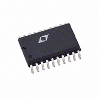
LT1795CSW#TR Linear Technology, LT1795CSW#TR Datasheet - Page 9

LT1795CSW#TR
Manufacturer Part Number
LT1795CSW#TR
Description
IC AMP CURR FEEDBACK DUAL 20SOIC
Manufacturer
Linear Technology
Datasheet
1.LT1795CSW.pdf
(12 pages)
Specifications of LT1795CSW#TR
Amplifier Type
Current Feedback
Number Of Circuits
2
Slew Rate
900 V/µs
-3db Bandwidth
65MHz
Current - Input Bias
10µA
Voltage - Input Offset
3000µV
Current - Supply
29mA
Current - Output / Channel
1A
Voltage - Supply, Single/dual (±)
±5 V ~ 15 V
Operating Temperature
0°C ~ 70°C
Mounting Type
Surface Mount
Package / Case
20-SOIC (7.5mm Width)
Lead Free Status / RoHS Status
Contains lead / RoHS non-compliant
Output Type
-
Gain Bandwidth Product
-
Lead Free Status / Rohs Status
Not Compliant
Available stocks
Company
Part Number
Manufacturer
Quantity
Price
APPLICATIO S I FOR ATIO
ture until the device begins thermal shutdown gives a
good indication of how much margin there is in the
thermal design.
For surface mount devices, heat sinking is accomplished
by using the heat spreading capabilities of the PC board
and its copper traces. For the TSSOP package, power is
dissipated through the exposed heatsink. For the SO
package, power is dissipated from the package primarily
through the V
should have a good thermal connection to a copper plane,
either by direct contact or by plated through holes. The
copper plane may be an internal or external layer. The
thermal resistance, junction-to-ambient will depend on
the total copper area connected to the device. For example,
the thermal resistance of the LT1795 connected to a 2 2
inch, double sided 2 oz copper plane is 40 C/W.
CALCULATING JUNCTION TEMPERATURE
The junction temperature can be calculated from the
equation:
where
Differential Input Signal Swing
The differential input swing is limited to about 5V by an
ESD protection device connected between the inputs. In
normal operation, the differential voltage between the
input pins is small, so this clamp has no effect. However,
in the shutdown mode, the differential swing can be the
same as the input swing. The clamp voltage will then set
the maximum allowable input voltage.
POWER SUPPLY BYPASSING
To obtain the maximum output and the minimum distor-
tion from the LT1795, the power supply rails should be
well bypassed. For example, with the output stage supply-
T
T
T
P
J
J
A
JA
D
= (P
= Junction Temperature
= Ambient Temperature
= Device Dissipation
= Thermal Resistance (Junction-to-Ambient)
D
)(
JA
–
) + T
pins (4 to 7 and 14 to 17). These pins
U
A
U
W
U
ing 0.5A current peaks into the load, a 1 power supply
impedance will cause a droop of 0.5V, reducing the
available output swing by that amount. Surface mount
tantalum and ceramic capacitors make excellent low ESR
bypass elements when placed close to the chip. For
frequencies above 100kHz, use 1 F and 100nF ceramic
capacitors. If significant power must be delivered below
100kHz, capacitive reactance becomes the limiting factor.
Larger ceramic or tantalum capacitors, such as 4.7 F, are
recommended in place of the 1 F unit mentioned above.
Inadequate bypassing is evidenced by reduced output
swing and “distorted” clipping effects when the output is
driven to the rails. If this is observed, check the supply pins
of the device for ripple directly related to the output
waveform. Significant supply modulation indicates poor
bypassing.
Capacitance on the Inverting Input
Current feedback amplifiers require resistive feedback
from the output to the inverting input for stable operation.
Take care to minimize the stray capacitance between the
output and the inverting input. Capacitance on the invert-
ing input to ground will cause peaking in the frequency
response (and overshoot in the transient response), but it
does not degrade the stability of the amplifier.
Feedback Resistor Selection
The optimum value for the feedback resistors is a function
of the operating conditions of the device, the load imped-
ance and the desired flatness of response. The Typical AC
Performance tables give the values which result in less
than 1dB of peaking for various resistive loads and oper-
ating conditions. If this level of flatness is not required, a
higher bandwidth can be obtained by use of a lower
feedback resistor.
For resistive loads, the COMP pin should be left open (see
Capacitive Loads section).
Capacitive Loads
The LT1795 includes an optional compensation network
for driving capacitive loads. This network eliminates most
of the output stage peaking associated with capacitive
loads, allowing the frequency response to be flattened.
LT1795
1795fa
9


