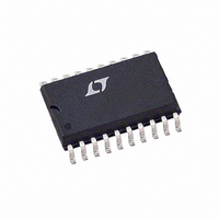
LT1795CSW#TR Linear Technology, LT1795CSW#TR Datasheet - Page 2

LT1795CSW#TR
Manufacturer Part Number
LT1795CSW#TR
Description
IC AMP CURR FEEDBACK DUAL 20SOIC
Manufacturer
Linear Technology
Datasheet
1.LT1795CSW.pdf
(12 pages)
Specifications of LT1795CSW#TR
Amplifier Type
Current Feedback
Number Of Circuits
2
Slew Rate
900 V/µs
-3db Bandwidth
65MHz
Current - Input Bias
10µA
Voltage - Input Offset
3000µV
Current - Supply
29mA
Current - Output / Channel
1A
Voltage - Supply, Single/dual (±)
±5 V ~ 15 V
Operating Temperature
0°C ~ 70°C
Mounting Type
Surface Mount
Package / Case
20-SOIC (7.5mm Width)
Lead Free Status / RoHS Status
Contains lead / RoHS non-compliant
Output Type
-
Gain Bandwidth Product
-
Lead Free Status / Rohs Status
Not Compliant
Available stocks
Company
Part Number
Manufacturer
Quantity
Price
PACKAGE/ORDER I FOR ATIO
LT1795
ABSOLUTE AXI U RATI GS
Supply Voltage ...................................................... 18V
Input Current ...................................................... 15mA
Output Short-Circuit Duration (Note 2) ............ Indefinite
Operating Temperature Range ................ – 40 C to 85 C
Consult LTC Marketing for parts specified with wider operating temperature ranges.
SYMBOL
V
I
I
e
+ i
– i
ELECTRICAL CHARACTERISTICS
The
V
2
IN
IN
n
OS
CM
n
n
+
–
UNDERSIDE METAL INTERNALLY CONNECTED TO V
SHDNREF
= 0V, 5V V
denotes the specifications which apply over the full specified temperature range, otherwise specifications are at T
SHDN
T
–IN
–IN
+IN
+IN
NC
NC
JMAX
V
V
–
–
(PCB CONNECTION OPTIONAL)
20-LEAD PLASTIC TSSOP
10
= 150 C,
1
2
3
4
5
6
7
8
9
PARAMETER
Input Offset Voltage
Input Offset Voltage Matching
Input Offset Voltage Drift
Noninverting Input Current
Noninverting Input Current Matching
Inverting Input Current
Inverting Input Current Matching
Input Noise Voltage Density
Input Noise Current Density
Input Noise Current Density
FE PACKAGE
TOP VIEW
S
JA
W
= 40 C/W (Note 4)
15V, pulse tested, V
20
19
18
17
16
15
14
13
12
11
V
NC
OUT
V
COMP
COMP
V
OUT
NC
V
W W
–
+
+
–
U
–
SHDN
ORDER PART
W
LT1795CFE
LT1795IFE
= 2.5V, V
NUMBER
U
CONDITIONS
f = 10kHz, R
f = 10kHz, R
f = 10kHz, R
SHDNREF
U
(Note 1)
F
F
F
=1k, R
=1k, R
=1k, R
= 0V unless otherwise noted. (Note 3)
Specified Temperature Range (Note 3) ... – 40 C to 85 C
Junction Temperature ........................................... 150 C
Storage Temperature Range ................. – 65 C to 150 C
Lead Temperature (Soldering, 10 sec).................. 300 C
G
G
G
= 10 , R
= 10 , R
= 10 , R
COMP
SHDN
OUT
–IN
+IN
V
V
V
V
V
T
+
–
–
–
–
JMAX
10
1
2
3
4
5
6
7
8
9
= 150 C,
S
S
S
20-LEAD PLASTIC SW
= 0
= 10k
= 10k
S PACKAGE
TOP VIEW
JA
40 C/W (Note 4)
20
19
18
17
16
15
14
13
12
11
COMP
V
OUT
V
V
V
V
–IN
+IN
SHDNREF
+
–
–
–
–
MIN
TYP
3.6
10
30
1.5
1.5
4.5
0.5
10
10
2
20
20
1
3
2
8
ORDER PART
LT1795CSW
LT1795ISW
NUMBER
MAX
A
100
3.5
5.0
13
17
20
70
30
50
5
2
7
= 25 C.
nV/ Hz
pA/ Hz
pA/ Hz
UNITS
1795fa
V/ C
mV
mV
mV
mV
A
A
A
A
A
A
A
A


