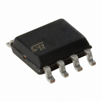
TSV992ID STMicroelectronics, TSV992ID Datasheet

TSV992ID
Specifications of TSV992ID
Available stocks
Related parts for TSV992ID
TSV992ID Summary of contents
Page 1
Rail-to-rail input/output 20 MHz GBP operational amplifiers Features ■ Low input offset voltage: 1.5 mV max (A grade) ■ Rail-to-rail input and output ■ Wide bandwidth 20 MHz, stable for gain ■ Low power consumption: 820 µA typ ■ High ...
Page 2
Absolute maximum ratings and operating conditions 1 Absolute maximum ratings and operating conditions Table 1. Absolute maximum ratings Symbol V Supply voltage CC V Differential input voltage id V Input voltage in I Input current in T Storage temperature stg ...
Page 3
TSV99x-TSV99xA Table 2. Operating conditions Symbol V Supply voltage CC V Common mode input voltage range icm T Operating free air temperature range op Absolute maximum ratings and operating conditions Parameter Doc ID 12833 Rev 8 Value Unit 2.5 to ...
Page 4
Electrical characteristics 2 Electrical characteristics Table 3. Electrical characteristics /2, full temperature range (unless otherwise specified) CC Symbol Parameter DC performance Offset voltage TSV99x V io TSV99xA DV Input offset voltage drift io (2) Input offset ...
Page 5
TSV99x-TSV99xA Table 4. Electrical characteristics /2, full temperature range (unless otherwise specified) CC Symbol Parameter DC performance Offset voltage TSV99x V io TSV99xA DV Input offset voltage drift io (2) Input offset current ...
Page 6
Electrical characteristics Table 5. Electrical characteristics connected Symbol Parameter DC performance Offset voltage TSV99x V io TSV99xA DV Input offset voltage drift io (2) Input offset current /2) out ...
Page 7
TSV99x-TSV99xA Figure 1. Input offset voltage distribution 25° C 140 120 100 Input offset Voltage (mV) Figure 3. Supply current vs. input common mode voltage at ...
Page 8
Electrical characteristics Figure 7. Voltage gain and phase vs frequency 0.5 V icm Figure 9. Positive slew rate Vin : from 0.5V to Vcc-0. calculated from 10% to 90% Figure 11. Distortion + ...
Page 9
TSV99x-TSV99xA Figure 13. Noise vs. frequency Figure 14. Supply current vs. supply voltage Doc ID 12833 Rev 8 Electrical characteristics 9/20 ...
Page 10
Application information 3 Application information 3.1 Driving resistive and capacitive loads These products are low-voltage, low-power operational amplifiers optimized to drive rather large resistive loads above 2 kΩ . The TSV99x are not unity gain stable. To ensure proper stability ...
Page 11
... TSV99x-TSV99xA 3.3 Macromodel An accurate macromodel of the TSV99x is available on STMicroelectronics’ web site at www.st.com. This model is a trade-off between accuracy and complexity (that is, time simulation) of the TSV99x operational amplifiers. It emulates the nominal performances of a typical device within the specified operating conditions mentioned in the datasheet. It helps to validate a design approach and to select the right operational amplifier, but it does not replace on-board measurements ...
Page 12
Package information 4 Package information In order to meet environmental requirements, ST offers these devices in different grades of ® ECOPACK packages, depending on their level of environmental compliance. ECOPACK specifications, grade definitions and product status are available at: www.st.com. ...
Page 13
TSV99x-TSV99xA 4.1 SOT23-5 package information Figure 17. SOT23-5 package mechanical drawing Table 6. SOT23-5 package mechanical data Ref degrees Dimensions Millimeters Min. Typ. Max. 0.90 1.20 1.45 ...
Page 14
Package information 4.2 MiniSO-8 package information Figure 18. MiniSO-8 package mechanical drawing Table 7. MiniSO-8 package mechanical data Ref ccc 14/20 Dimensions Millimeters Min. Typ. Max. 1.1 ...
Page 15
TSV99x-TSV99xA 4.3 SO-8 package information Figure 19. SO-8 package mechanical drawing Table 8. SO-8 package mechanical data Ref ccc Dimensions Millimeters Min. Typ. Max. 1.75 0.10 0.25 ...
Page 16
Package information 4.4 TSSOP14 package information Figure 20. TSSOP14 package mechanical drawing Table 9. TSSOP14 package mechanical data Ref aaa 16/20 Dimensions Millimeters Min. Typ. Max. 1.20 0.05 ...
Page 17
TSV99x-TSV99xA 4.5 SO-14 package information Figure 21. SO-14 package mechanical drawing Table 10. SO-14 package mechanical data Ref ddd Dimensions Millimeters Min. Typ. Max. 1.35 1.75 0.10 0.25 ...
Page 18
... Ordering information 5 Ordering information Table 11. Order codes Order code TSV991ILT TSV991AILT TSV992IST TSV992AIST TSV992ID TSV992IDT TSV992AID TSV992AIDT TSV994IPT TSV994AIPT TSV994ID TSV994IDT TSV994AID TSV994AIDT (2) TSV991IYLT (2) TSV991AIYLT (2) TSV992IYDT (2) TSV992AIYDT (2) TSV992IYST (2) TSV992AIYST (2) TSV994IYDT (2) TSV994AIYDT (2) TSV994IYPT (2) TSV994AIYPT 1. All packages are Moisture Sensitivity Level 1 as per Jedec J-STD-020-C, except SO-14 which is Jedec level 3 ...
Page 19
TSV99x-TSV99xA 6 Revision history Table 12. Document revision history Date 31-Jul-2006 07-Nov-2006 12-Dec-2006 07-Jun-2007 11-Feb-2008 25-May-2009 19-Oct-2009 14-Jan-2010 Revision 1 Preliminary data release for product under development. 2 Final version of datasheet. 3 Noise and distortion figures added. ESD tolerance ...
Page 20
... Information in this document is provided solely in connection with ST products. STMicroelectronics NV and its subsidiaries (“ST”) reserve the right to make changes, corrections, modifications or improvements, to this document, and the products and services described herein at any time, without notice. All ST products are sold pursuant to ST’s terms and conditions of sale. ...


