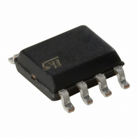
TS613IDT STMicroelectronics, TS613IDT Datasheet - Page 8

TS613IDT
Manufacturer Part Number
TS613IDT
Description
IC AMP DUAL WIDE BAND OP 8 SOIC
Manufacturer
STMicroelectronics
Datasheet
1.TS613ID.pdf
(10 pages)
Specifications of TS613IDT
Amplifier Type
Voltage Feedback
Number Of Circuits
2
Slew Rate
40 V/µs
Gain Bandwidth Product
130MHz
Current - Input Bias
5µA
Voltage - Input Offset
1000µV
Current - Supply
11mA
Current - Output / Channel
320mA
Voltage - Supply, Single/dual (±)
5 V ~ 12 V, ±2.5 V ~ 6 V
Operating Temperature
-40°C ~ 85°C
Mounting Type
Surface Mount
Package / Case
8-SOIC (3.9mm Width)
Number Of Channels
2
Voltage Gain Db
80.83 dB
Common Mode Rejection Ratio (min)
90 dB
Input Offset Voltage
6 mV
Supply Current
22 mA
Maximum Power Dissipation
2000 mW
Maximum Operating Temperature
+ 85 C
Mounting Style
SMD/SMT
Maximum Dual Supply Voltage
+/- 6 V
Minimum Operating Temperature
- 40 C
Power Supply Requirement
Single/Dual
Pin Count
8
Lead Free Status / RoHS Status
Lead free / RoHS Compliant
Output Type
-
-3db Bandwidth
-
Lead Free Status / Rohs Status
Details
Other names
497-2302-2
Available stocks
Company
Part Number
Manufacturer
Quantity
Price
Part Number:
TS613IDT
Manufacturer:
ST
Quantity:
20 000
TS613
By identification of both equations (2) and (3), the
synthesized impedance is, with Rs1=Rs2=Rs:
Figure 5 : Equivalent schematic. Ro is the syn-
Unlike the level Vo° required for a passive imped-
ance, Vo° will be smaller than 2Vo in our case. Let
us write Vo°=kVo with k the matching factor vary-
ing between 1 and 2. Assuming that the current
through R3 is negligeable, it comes the following
resistance divider:
After choosing the k factor, Rs will equal to
1/2RL(k-1).
A good impedance matching assumes:
From (4) and (5) it becomes:
By fixing an arbitrary value for R2, (6) gives:
Finally, the values of R2 and R3 allow us to extract
R1 from (1), and it comes:
with GL the required gain.
8/10
Vi.Gi
thesized impedance
R1
=
--------------------------------------------------------- 7
2 1
Ro
R2
------ -
R3
Ro
Ro
R o
R3
–
=
=
=
R2
------ -
R3
=
=
1
---------------------------
RL
---------------- - 4
1
Iout
1
-- - RL 5
2
2R2
–
-------------------
1
kVoRL
–
Rs
GL 1
+
2Rs
--------- - 6
–
R2
------ -
R3
RL
R2
2Rs1
2Rs
--------- -
,
RL
–
,
,
–
R2
------ -
R3
,
1/2
RL
CAPABILITIES
The table below shows the calculated compo-
nents
R2=1000
displays the maximum amplitude level on the line
regarding the TS613 maximum output capabilities
(18Vpp diff.) and a 1:2 line transformer ratio.
MEASUREMENT OF THE POWER
CONSUMPTION IN THE ADSL APPLICATION
Conditions:
Passive impedance matching
Transformer turns ratio: 2
Power Supply: 12V
Maximun level required on the line: 12.4Vpp
Maximum output level of the driver: 12.4Vpp
Crest factor: 5.3 (Vp/Vrms)
The TS613 power consumption during emission
on 900 and 4550 meter twisted pair telephone
lines: 360mW
GL (gain for the
loaded system)
1.3
1.4
1.5
1.6
1.7
k
R2 (=R4)
R3 (=R5)
Passive matching
Active matching
R1
Rs
820
490
360
270
240
( )
R1
for different values of k. In this case
and the gain=16dB. The last column
1500
1600
2200
2400
3300
( )
R3
GL is fixed for the application requirements
GL=Vo/Vi=0.5(1+2R2/R1+R2/R3)/(1-R2/R3)
2R2/[2(1-R2/R3)GL-1-R2/R3]
Abritrary fixed
R2/(1-Rs/0.5RL)
0.5RL(k-1)
( )
3.9
5.1
6.2
7.5
9.1
Rs
TS613 Output
Level to get
12.4Vpp on
(Vpp diff)
the line
10.5
12.4
8.7
9.3
9.9
8
Maximum
Line level
(Vpp diff)
27.5
25.7
25.3
23.7
22.3
18


