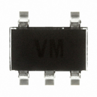
STM6322TWY6F STMicroelectronics, STM6322TWY6F Datasheet - Page 22

STM6322TWY6F
Manufacturer Part Number
STM6322TWY6F
Description
IC SUPERVISOR PB 3.08V SOT23-5
Manufacturer
STMicroelectronics
Type
Simple Reset/Power-On Resetr
Datasheet
1.STM6321SWY6F.pdf
(29 pages)
Specifications of STM6322TWY6F
Number Of Voltages Monitored
1
Output
Open Drain, Push-Pull
Reset
Active High/Active Low
Reset Timeout
140 ms Minimum
Voltage - Threshold
3.08V
Operating Temperature
-40°C ~ 85°C
Mounting Type
Surface Mount
Package / Case
SOT-23-5, SC-74A, SOT-25
Monitored Voltage
2.5 V or 3 V or 3.3 V or 5 V
Undervoltage Threshold
3.04 V
Overvoltage Threshold
3.11 V
Manual Reset
Resettable
Watchdog
No
Battery Backup Switching
No
Power-up Reset Delay (typ)
280 ms
Supply Voltage (max)
5.5 V
Supply Voltage (min)
1 V
Supply Current (typ)
12 uA
Maximum Power Dissipation
320 mW
Mounting Style
SMD/SMT
Maximum Operating Temperature
+ 85 C
Chip Enable Signals
No
Minimum Operating Temperature
- 40 C
Output Type
Active High or Active Low or Open Drain or Push-Pull
Power Fail Detection
No
Lead Free Status / RoHS Status
Lead free / RoHS Compliant
Other names
497-4798-2
Available stocks
Company
Part Number
Manufacturer
Quantity
Price
Company:
Part Number:
STM6322TWY6F
Manufacturer:
STMicroelectronics
Quantity:
1 300
Part Number:
STM6322TWY6F
Manufacturer:
ST
Quantity:
20 000
Package mechanical data
Table 6.
1. Valid for ambient operating temperature: T
2. V
3. WDI input is designed to be driven by a three-state output device. To float WDI, the “high-impedance mode” of the output
4. WDI is internally serviced within the watchdog period if WDI is left unconnected.
5. The leakage current measured on the RST pin is tested with the reset asserted (output high impedance).
6. Other t
7.
22/29
Push-button reset input
Watchdog timer
t
t
t
WD
Sym
MLMH
MLRL
“T/S/R” versions; and V
device must have a maximum leakage current of 10 µA and a maximum output capacitance of 200 pF. The output device
must also be able to source and sink at least 200 µA when active.
For V
CC
(6)
(min) = 1.0 V for T
CC
native
rec
Alter-
t
t
MRD
MR
< 3.0 V, t
and watchdog timings are offered. Minimum order quantities may apply. Contact local sales office for availability.
DC and AC characteristic (continued)
Watchdog timeout period
MR to RST output delay
WD
temperature coefficient
WDI pulse width
MR glitch immunity
MR pull-up resistor
(min) = 100 ns.
Reset threshold
A
MR pulse width
CC
Description
= 0 to +85 °C.
= 1.2 to 2.75 V for “Z/Y” version (except where noted).
(7)
A
= –40 to 85 °C; V
Doc ID 11110 Rev 10
Test condition
V
CC
CC
= 4.5 to 5.5 V for “L/M” versions; V
STM6321/6322STM6821/6822/6823/6824/6825
≥ 3.0 V
(1)
1.12
Min
35
50
1
CC
1.60
Typ
500
100
40
52
= 2.7 to 3.6 V for
Max
2.24
75
ppm/
Unit
kΩ
µs
ns
ns
ns
C
s


