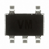
STM6717TWWY6F STMicroelectronics, STM6717TWWY6F Datasheet - Page 21

STM6717TWWY6F
Manufacturer Part Number
STM6717TWWY6F
Description
SUPERVISOR DUAL/TRPL PP SOT23-5
Manufacturer
STMicroelectronics
Type
Multi-Voltage Supervisorr
Datasheet
1.STM6717SFWY6F.pdf
(30 pages)
Specifications of STM6717TWWY6F
Number Of Voltages Monitored
2
Output
Open Drain or Open Collector
Reset
Active Low
Reset Timeout
140 ms Minimum
Voltage - Threshold
1.665V, 3.075V
Operating Temperature
-40°C ~ 85°C
Mounting Type
Surface Mount
Package / Case
SOT-23-5, SC-74A, SOT-25
Monitored Voltage
0.8 V to 5.5 V
Undervoltage Threshold
3 V or 1.62 V
Overvoltage Threshold
3.15 V or 1.71 V
Manual Reset
Resettable
Watchdog
No
Battery Backup Switching
No
Power-up Reset Delay (typ)
280 ms
Supply Voltage (max)
5.5 V
Supply Voltage (min)
0.8 V
Supply Current (typ)
35 uA
Maximum Power Dissipation
654 mW
Mounting Style
SMD/SMT
Maximum Operating Temperature
+ 85 C
Chip Enable Signals
No
Minimum Operating Temperature
- 40 C
Output Type
Active Low or Open Drain
Power Fail Detection
No
Lead Free Status / RoHS Status
Lead free / RoHS Compliant
Other names
497-5011-2
Available stocks
Company
Part Number
Manufacturer
Quantity
Price
Company:
Part Number:
STM6717TWWY6F
Manufacturer:
ST
Quantity:
3 918
Company:
Part Number:
STM6717TWWY6F
Manufacturer:
STMicroelectronics
Quantity:
2 400
STM6717/6718/6719/6720/STM6777/6778/6779/6780
Table 6.
1. Valid for ambient operating temperature: T
2. Input leakage for the MRC pin is not tested.
3. Guaranteed by design.
4. The leakage current measured on the RST pin is tested with the reset de-asserted (output high impedance).
5. Selecting the appropriate external capacitor (preferably less than 100 pF) allows systems designers to vary the minimum
Table 7.
1. At 25 °C (typical)
Manual (push-button) reset input
t
t
Sym
MLMH
MLRL
V
noted).
delay from 6µs (MRC pin left open) or more (see
V
IH
IL
V
1.6 V
2.0 V
3.0 V
4.0 V
5.0 V
CC1
native
Alter-
t
t
MRD
MR
DC and AC characteristics (continued)
t
MLMH
MR minimum pulse width
MR minimum pulse width
MR to RST output delay
100 pF
120 µs
122 µs
125 µs
128 µs
130 µs
minimum pulse width
MR pull-up resistance
(STM6717/18/19/20)
(STM6777/78/79/80)
(STM6717/18/19/20)
MR glitch immunity
MR input voltage
Description
120 ms
122 ms
125 ms
129 ms
130 ms
0.1 µF
A
= –40 to 85 °C; V
Table
Doc ID 11469 Rev 7
7).
2.2 µF
MRC connected via
2.6 s
2.7 s
2.7 s
2.8 s
2.8 s
capacitor to V
Test condition
Capacitor value
CC1
= 0.8 to 5.5 V and V
SS
3.3 µF
(1)
4.0 s
4.0 s
4.1 s
4.2 s
4.3 s
(5)
(1)
CC2
= 0.8 to 3.6 V (except where
0.7V
Min
25
1
4.7 µF
DC and AC parameters
CC1
5.6 s
5.8 s
5.9 s
6.0 s
6.1 s
Typ
200
100
50
6
0.3V
Max
80
C1
6.8 µF
8.2 s
8.3 s
8.5 s
8.7 s
8.8 s
C
21/30
Unit
kΩ
µs
µs
ns
ns
V
V


