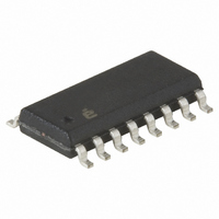
X40235S16I-BT1 Intersil, X40235S16I-BT1 Datasheet - Page 18

X40235S16I-BT1
Manufacturer Part Number
X40235S16I-BT1
Description
IC VOLTAGE MON TRPL EE 16-SOIC
Manufacturer
Intersil
Type
Multi-Voltage Supervisorr
Datasheet
1.X40231S16I-A.pdf
(36 pages)
Specifications of X40235S16I-BT1
Number Of Voltages Monitored
3
Output
Open Drain, Open Drain
Reset
Active High/Active Low
Reset Timeout
Adjustable/Selectable
Voltage - Threshold
1.75V, 2.95V, 4.45V
Operating Temperature
-40°C ~ 85°C
Mounting Type
Surface Mount
Package / Case
16-SOIC (0.300", 7.5mm Width)
Lead Free Status / RoHS Status
Contains lead / RoHS non-compliant
CONTROL AND STATUS REGISTER
The Control and Status (CR) Register provides the user
with a mechanism for changing and reading the status
of various parameters of the X4023x (See Figure 17).
The CR register is a combination of both volatile and
nonvolatile bits. The nonvolatile bits of the CR register
retain their stored values even when V
down, then powered back up. The volatile bits how-
ever, will always power-up to a known logic state “0”
(irrespective of their value at power-down).
A detailed description of the function of each of the CR
register bits follows:
WEL: Write Enable Latch (Volatile)
The WEL bit controls the Write Enable status of the
entire X4023x device. This bit must first be enabled
before ANY write operation (to DCPs, EEPROM mem-
ory array, or the CR register). If the WEL bit is not first
enabled, then ANY proceeding (volatile or nonvolatile)
write operation to DCPs, EEPROM array, as well as
the CR register, is aborted and no ACKNOWLEDGE is
issued after a Data Byte.
The WEL bit is a volatile latch that powers up in the
disabled, LOW (0) state. The WEL bit is enabled / set
by writing 00000010 to the CR register. Once enabled,
the WEL bit remains set to “1” until either it is reset to
“0” (by writing 00000000 to the CR register) or until the
X4023x powers down, and then up again.
Writes to the WEL bit do not cause an internal high
voltage write cycle. Therefore, the device is ready for
another operation immediately after a STOP condition
is executed in the CR Write command sequence (See
Figure 18).
NOTE: Bits labelled NV are nonvolatile (See “CONTROL AND STATUS REGISTER”).
PUP1 - PUP0
PUP1
NV
CS7
BL1 - BL0
RWEL
Bit(s)
V2FS
V3FS
WEL
V2FS
Figure 17. CR Register Format
CS6
V3FS
CS5
Register Write Enable Latch bit
Sets the Power-on Reset time
CS4
Sets the Block Lock partition
BL1
V2MON Output Flag Status
V3MON Output Flag Status
NV
Write Enable Latch bit
18
BL0
CS3
Description
NV
X40231, X40233, X40235, X40237, X40239
CS2
RWEL
CS1
CC
WEL
is powered
PUP0
CS0
NV
RWEL: Register Write Enable Latch (Volatile)
The RWEL bit controls the (CR) Register Write Enable
status of the X4023x. Therefore, in order to write to
any of the bits of the CR Register (except WEL), the
RWEL bit must first be set to “1”. The RWEL bit is a
volatile bit that powers up in the disabled, LOW (“0”)
state.
It must be noted that the RWEL bit can only be set,
once the WEL bit has first been enabled (See "CR
Register Write Operation").
The RWEL bit will reset itself to the default “0” state, in
one of three cases:
—After a successful write operation to any bits of the CR
—When the X4023x is powered down.
—When attempting to write to a Block Lock protected
BL1, BL0: Block Lock protection bits - (Nonvolatile)
The Block Lock protection bits (BL1 and BL0) are used
to:
—Inhibit a write operation from being performed to cer-
—Inhibit a DCP write operation (changing the “wiper
The region of EEPROM memory which is protected /
locked is determined by the combination of the BL1
and BL0 bits written to the CR register. It is possible to
lock the regions of EEPROM memory shown in the
table below:
If the user attempts to perform a write operation on a
protected region of EEPROM memory, the operation
is aborted without changing any data in the array.
BL1 BL0
0
0
1
1
register has been completed (See Figure 18).
region of the EEPROM memory (See "BL1, BL0: Block
Lock protection bits - (Nonvolatile)", below).
tain addresses of the EEPROM memory array
position”).
0
1
0
1
Protected Addresses
80
00
C0
None (Default)
h
h
h
- FF
- FF
- FF
(Size)
h
h
h
(128 bytes
(256 bytes)
(64 bytes
)
)
Partition of array
None (Default)
Upper 1/4
Upper 1/2
locked
All
April 11, 2005
FN8115.0


