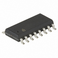
X40235S16I-BT1 Intersil, X40235S16I-BT1 Datasheet - Page 29

X40235S16I-BT1
Manufacturer Part Number
X40235S16I-BT1
Description
IC VOLTAGE MON TRPL EE 16-SOIC
Manufacturer
Intersil
Type
Multi-Voltage Supervisorr
Datasheet
1.X40231S16I-A.pdf
(36 pages)
Specifications of X40235S16I-BT1
Number Of Voltages Monitored
3
Output
Open Drain, Open Drain
Reset
Active High/Active Low
Reset Timeout
Adjustable/Selectable
Voltage - Threshold
1.75V, 2.95V, 4.45V
Operating Temperature
-40°C ~ 85°C
Mounting Type
Surface Mount
Package / Case
16-SOIC (0.300", 7.5mm Width)
Lead Free Status / RoHS Status
Contains lead / RoHS non-compliant
D.C. OPERATING CHARACTERISTICS
Notes: 1. The device enters the Active state after any START, and remains active until: 9 clock cycles later if the Device Select Bits in the Slave
Notes: 2. The device goes into Standby: 200nS after any STOP, except those that initiate a high voltage write cycle; t
Notes: 3. Current through external pull up resistor not included.
Notes: 4. V
Notes: 5. V
Notes: 6. See “ORDERING INFORMATION” on page 36.
Notes: 7. V
Notes: 8. Equivalent input circuit for V
V
I
I
I
I
V
V
V
V
V
t
I
V
V
V
CC
CC
LI
LO
RPDx
Vx
CC
TRIP1PR
TRIPx
TRIP1
TRIP2
TRIP3
IL
IH
OLx
Symbol
(7)
(7)
1
2
(1)
(2)
(6)
(6)
(6)
PR
Address Byte are incorrect; 200nS after a STOP ending a read operation; or t
a high voltage cycle; or 9 clock cycles after any START that is not followed by the correct Device Select Bits in the Slave Address Byte.
IN
OUT
IL
Min. and V
= Voltage applied to input pin.
= Voltage applied to output pin.
Current into V
Read memory array
Write nonvolatile memory V
Current into V
With 2-Wire bus activity
No 2-Wire bus activity
V
Input Leakage Current
Input Leakage Current
Output Leakage Current
V2FAIL
V
V
Pre - programmed V
Pre - programmed V
Pre - programmed V
V
V2FAIL
delay (respectively)
V2MON Input leakage current
V3MON Input leakage current
Input LOW Voltage (SCL, SDA, WP, MR)
Input HIGH Voltage (SCL,SDA, WP, MR)
RESET,
Low Voltage
CC
TRIP1
TRIPx
CC
IH
, V2MON, V3MON to RESET,
= 3.5V
Max. are for reference only and are not tested
Programming Range
Programming Range (x = 2,3)
,
,
V2FAIL
V3FAIL
V3FAIL
29
CC
CC
Parameter
XMON
,
Pin (X4023x: Active)
Pin (X4023x:Standby)
)
X40231, X40233, X40235, X40237, X40239
propagation
V3FAIL
TRIP1
TRIP2
TRIP3
(3)
(SCL, SDA, MR)
(WP)
(3)
(SDA, RESET,
threshold
threshold
threshold
, SDA Output
CC
V
XMON
= 3.5V
2.75
1.75
2.05
1.60
1.60
-0.5
Min
2.7
2.8
4.3
2.8
2.0
V
REF
2.95
4.45
2.20
2.95
1.75
1.75
Typ
0.1
0.1
+
–
WC
Max
50.0
50.0
4.70
3.50
3.00
4.50
2.25
3.00
1.80
1.80
V
+0.5
5.5
0.4
1.5
0.8
0.4
10
10
10
20
CC
1
1
after a STOP ending a write operation.
Unit
mA
µA
µA
µA
µA
µA
µs
V
V
V
V
V
V
V
V
V
Requires V
not operate.
f
V
MR = VSS
WP = VSS or Open/Floating
V
activity else f
V
V
X4023x is in Standby
Factory shipped default option A
Factory shipped default option B
Factory shipped default option A
Factory shipped default option B
Factory shipped default option A
Factory shipped default option B
V
Others = GND or V
I
SCL
SINK
SDA
SCL
IN
OUT
SDA
(4)
Test Conditions / Notes
= 400KHz
= V
(5)
= V
= 2.0mA
= V
= GND to V
= GND to V
CC
SCL
CC
WC
CC
(when no bus
after a STOP that initiates
SCL
= V
See
> V
CC
= 400kHz)
TRIP1
CC
(8)
CC
CC
.
(2)
.
or chip will
April 11, 2005
FN8115.0


