MCP1700-3002E/TO Microchip Technology, MCP1700-3002E/TO Datasheet - Page 10
MCP1700-3002E/TO
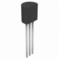
Manufacturer Part Number
MCP1700-3002E/TO
Description
IC REG LDO 250MA 3.0V TO-92-3
Manufacturer
Microchip Technology
Datasheet
1.SOT89-3EV-VREG.pdf
(24 pages)
Specifications of MCP1700-3002E/TO
Package / Case
TO-92-3 (Standard Body), TO-226
Regulator Topology
Positive Fixed
Voltage - Output
3V
Voltage - Input
Up to 6V
Voltage - Dropout (typical)
0.178V @ 250mA
Number Of Regulators
1
Current - Output
250mA (Min)
Operating Temperature
-40°C ~ 125°C
Mounting Type
Through Hole
Number Of Outputs
1
Polarity
Positive
Input Voltage Max
6 V
Output Voltage
3 V
Output Type
Fixed
Dropout Voltage (max)
350 mV
Output Current
250 mA
Line Regulation
0.75 % / V
Load Regulation
1 %
Voltage Regulation Accuracy
3 %
Maximum Power Dissipation
0.644 W
Maximum Operating Temperature
+ 125 C
Mounting Style
Through Hole
Minimum Operating Temperature
- 40 C
Primary Input Voltage
4V
Output Voltage Fixed
3V
Dropout Voltage Vdo
178mV
No. Of Pins
3
Voltage Regulator Case Style
TO-92
Operating Temperature Range
-40°C To +125°C
Rohs Compliant
Yes
Lead Free Status / RoHS Status
Lead free / RoHS Compliant
Current - Limit (min)
-
Lead Free Status / Rohs Status
Lead free / RoHS Compliant
Available stocks
Company
Part Number
Manufacturer
Quantity
Price

Part Number:
MCP1700-3002E/TO
Manufacturer:
MICROCHIP/微芯
Quantity:
20 000


MCP1700
3.0
The descriptions of the pins are listed in
TABLE 3-1:
3.1
Regulator ground. Tie GND to the negative side of the
output and the negative side of the input capacitor.
Only the LDO bias current (1.6 µA typical) flows out of
this pin; there is no high current. The LDO output
regulation is referenced to this pin. Minimize voltage
drops between this pin and the negative side of the
load.
3.2
Connect V
positive terminal of the output capacitor. The positive
side of the output capacitor should be physically
located as close to the LDO V
The current flowing out of this pin is equal to the DC
load current.
DS21826B-page 10
Pin No.
SOT-23
1
2
3
PIN DESCRIPTIONS
Ground Terminal (GND)
Regulated Output Voltage (V
OUT
to the positive side of the load and the
Pin No.
SOT-89
PIN FUNCTION TABLE
1
3
2
Pin No.
OUT
TO-92
1
3
2
pin as is practical.
Table
Name
V
OUT
3-1.
GND
V
OUT
IN
)
Ground Terminal
Regulated Voltage Output
Unregulated Supply Voltage
3.3
Connect V
Like all low dropout linear regulators, low source
impedance is necessary for the stable operation of the
LDO. The amount of capacitance required to ensure
low source impedance will depend on the proximity of
the input source capacitors or battery type. For most
applications, 1 µF of capacitance will ensure stable
operation of the LDO circuit. For applications that have
load currents below 100 mA, the input capacitance
requirement can be lowered. The type of capacitor
used
electrolytic. The low ESR characteristics of the ceramic
will yield better noise and PSRR performance at high
frequency.
can
Unregulated Input Voltage Pin
(V
IN
IN
be
to the input unregulated source voltage.
)
ceramic,
Function
© 2007 Microchip Technology Inc.
tantalum
or
aluminum
Related parts for MCP1700-3002E/TO
Image
Part Number
Description
Manufacturer
Datasheet
Request
R

Part Number:
Description:
IC REG LDO 250MA 1.2V TO-92-3
Manufacturer:
Microchip Technology
Datasheet:
Part Number:
Description:
IC LDO REG 250MA 1.8V TO-92-3
Manufacturer:
Microchip Technology
Datasheet:
Part Number:
Description:
IC REG LDO 250MA 2.5V TO-92-3
Manufacturer:
Microchip Technology
Datasheet:
Part Number:
Description:
IC LDO REG 250MA 5.0V TO-92-3
Manufacturer:
Microchip Technology
Datasheet:

Part Number:
Description:
250mA CMOS LDO, Isupply 1uA And 2% Vout Accuracy 3 TO-92 BAG
Manufacturer:
Microchip Technology
Datasheet:
Part Number:
Description:
IC LDO REG 250MA 3.3V TO-92-3
Manufacturer:
Microchip Technology
Datasheet:
Part Number:
Description:
IC LDO REG 250MA 1.5V TO-92-3
Manufacturer:
Microchip Technology
Datasheet:
Part Number:
Description:
250mA CMOS LDO, Isupply 1uA And 2% Vout Accuracy 3 TO-92 BAG
Manufacturer:
Microchip Technology
Datasheet:
Part Number:
Description:
250mA CMOS LDO, Isupply 1uA And 2% Vout Accuracy 3 TO-92 BAG
Manufacturer:
Microchip Technology
Datasheet:
Part Number:
Description:
250mA CMOS LDO, Isupply 1uA And 2% Vout Accuracy 3 TO-92 BAG
Manufacturer:
Microchip Technology
Datasheet:
Part Number:
Description:
250mA CMOS LDO, Isupply 1uA And 2% Vout Accuracy 3 TO-92 BAG
Manufacturer:
Microchip Technology
Datasheet:
Part Number:
Description:
250mA CMOS LDO, Isupply 1uA And 2% Vout Accuracy 3 TO-92 BAG
Manufacturer:
Microchip Technology
Datasheet:
Part Number:
Description:
250mA CMOS LDO, Isupply 1uA And 2% Vout Accuracy 3 TO-92 BAG
Manufacturer:
Microchip Technology
Datasheet:
Part Number:
Description:
250mA CMOS LDO, Isupply 1uA And 2% Vout Accuracy 3 TO-92 BAG
Manufacturer:
Microchip Technology
Datasheet:
Part Number:
Description:
250mA CMOS LDO, Isupply 1uA And 2% Vout Accuracy 3 TO-92 BAG
Manufacturer:
Microchip Technology
Datasheet: