MCP1700-3002E/TO Microchip Technology, MCP1700-3002E/TO Datasheet - Page 14
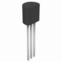
MCP1700-3002E/TO
Manufacturer Part Number
MCP1700-3002E/TO
Description
IC REG LDO 250MA 3.0V TO-92-3
Manufacturer
Microchip Technology
Datasheet
1.SOT89-3EV-VREG.pdf
(24 pages)
Specifications of MCP1700-3002E/TO
Package / Case
TO-92-3 (Standard Body), TO-226
Regulator Topology
Positive Fixed
Voltage - Output
3V
Voltage - Input
Up to 6V
Voltage - Dropout (typical)
0.178V @ 250mA
Number Of Regulators
1
Current - Output
250mA (Min)
Operating Temperature
-40°C ~ 125°C
Mounting Type
Through Hole
Number Of Outputs
1
Polarity
Positive
Input Voltage Max
6 V
Output Voltage
3 V
Output Type
Fixed
Dropout Voltage (max)
350 mV
Output Current
250 mA
Line Regulation
0.75 % / V
Load Regulation
1 %
Voltage Regulation Accuracy
3 %
Maximum Power Dissipation
0.644 W
Maximum Operating Temperature
+ 125 C
Mounting Style
Through Hole
Minimum Operating Temperature
- 40 C
Primary Input Voltage
4V
Output Voltage Fixed
3V
Dropout Voltage Vdo
178mV
No. Of Pins
3
Voltage Regulator Case Style
TO-92
Operating Temperature Range
-40°C To +125°C
Rohs Compliant
Yes
Lead Free Status / RoHS Status
Lead free / RoHS Compliant
Current - Limit (min)
-
Lead Free Status / Rohs Status
Lead free / RoHS Compliant
Available stocks
Company
Part Number
Manufacturer
Quantity
Price

Part Number:
MCP1700-3002E/TO
Manufacturer:
MICROCHIP/微芯
Quantity:
20 000


MCP1700
6.3
Internal power dissipation, junction temperature rise,
junction temperature and maximum power dissipation
are calculated in the following example. The power
dissipation, as a result of ground current, is small
enough to be neglected.
6.3.1
Device Junction Temperature Rise
The internal junction temperature rise is a function of
internal power dissipation and the thermal resistance
from junction to ambient for the application. The thermal
resistance from junction to ambient (Rθ
from an EIA/JEDEC standard for measuring thermal
resistance for small surface mount packages. The EIA/
JEDEC specification is JESD51-7, “High Effective
Thermal Conductivity Test Board for Leaded Surface
Mount Packages”. The standard describes the test
method and board specifications for measuring the
thermal resistance from junction to ambient. The actual
thermal resistance for a particular application can vary
depending on many factors, such as copper area and
thickness. Refer to AN792, “A Method to Determine
How Much Power a SOT-23 Can Dissipate in an
Application”, (DS00792), for more information regarding
this subject.
Junction Temperature Estimate
To estimate the internal junction temperature, the
calculated temperature rise is added to the ambient or
offset temperature. For this example, the worst-case
junction temperature is estimated below.
DS21826B-page 14
Package
Package Type = SOT-23
Input Voltage
LDO Output Voltages and Currents
Maximum Ambient Temperature
Internal Power Dissipation
Internal Power dissipation is the product of the LDO
output current times the voltage across the LDO
(V
IN
P
to V
T
LDO(MAX)
T
T
J(RISE)
T
JRISE
JRISE
A(MAX)
Voltage Regulator
OUT
V
P
P
I
OUT
OUT
LDO
LDO
POWER DISSIPATION EXAMPLE
V
IN
).
= P
= 218.1 milli-Watts x 230.0
= 50.2
= 2.3V to 3.2V
= 1.8V
= 150 mA
= +40°C
= (V
= (3.2V - (0.97 x 1.8V)) x 150 mA
= 218.1 milli-Watts
TOTAL
IN(MAX)
°
C
x Rq
- V
JA
OUT(MIN)
) x I
JA
°
C/Watt
) is derived
OUT(MAX)
Maximum Package Power Dissipation at +40°C
Ambient Temperature
6.4
The MCP1700 can be used not only as a regulator, but
also as a low quiescent current voltage reference. In
many microcontroller applications, the initial accuracy
of the reference can be calibrated using production test
equipment or by using a ratio measurement. When the
initial accuracy is calibrated, the thermal stability and
line regulation tolerance are the only errors introduced
by the MCP1700 LDO. The low cost, low quiescent
current and small ceramic output capacitor are all
advantages when using the MCP1700 as a voltage
reference.
FIGURE 6-2:
voltage reference.
6.5
For some applications, there are pulsed load current
events that may exceed the specified 250 mA
maximum specification of the MCP1700. The internal
current limit of the MCP1700 will prevent high peak
load demands from causing non-recoverable damage.
The 250 mA rating is a maximum average continuous
rating. As long as the average current does not exceed
250 mA, pulsed higher load currents can be applied to
the MCP1700
MCP1700 is 550 mA (T
SOT-23 (230.0°C/Watt = Rθ
SOT-89 (52°C/Watt = Rθ
TO-92 (131.9°C/Watt = Rθ
C
1 µF
IN
1 µA Bias
P
P
P
P
P
P
D(MAX)
D(MAX)
D(MAX)
D(MAX)
D(MAX)
D(MAX)
Bridge Sensor
Voltage Reference
Pulsed Load Applications
MCP1700
V
T
T
GND
IN
J
J
= T
= 90.2°C
= (125°C - 40°C) / 230°C/W
= 369.6 milli-Watts
= (125°C - 40°C) / 52°C/W
= 1.635 Watts
= (125°C - 40°C) / 131.9°C/W
= 644 milli-Watts
V
OUT
.
Ratio Metric Reference
The typical current limit for the
JRISE
C
1 µF
Using the MCP1700 as a
OUT
A
+ T
© 2007 Microchip Technology Inc.
+25°C).
JA
A(MAX)
JA
)
JA
)
)
V
ADO
AD1
Microcontroller
REF
PIC
®
Related parts for MCP1700-3002E/TO
Image
Part Number
Description
Manufacturer
Datasheet
Request
R

Part Number:
Description:
IC REG LDO 250MA 1.2V TO-92-3
Manufacturer:
Microchip Technology
Datasheet:
Part Number:
Description:
IC LDO REG 250MA 1.8V TO-92-3
Manufacturer:
Microchip Technology
Datasheet:
Part Number:
Description:
IC REG LDO 250MA 2.5V TO-92-3
Manufacturer:
Microchip Technology
Datasheet:
Part Number:
Description:
IC LDO REG 250MA 5.0V TO-92-3
Manufacturer:
Microchip Technology
Datasheet:

Part Number:
Description:
250mA CMOS LDO, Isupply 1uA And 2% Vout Accuracy 3 TO-92 BAG
Manufacturer:
Microchip Technology
Datasheet:
Part Number:
Description:
IC LDO REG 250MA 3.3V TO-92-3
Manufacturer:
Microchip Technology
Datasheet:
Part Number:
Description:
IC LDO REG 250MA 1.5V TO-92-3
Manufacturer:
Microchip Technology
Datasheet:
Part Number:
Description:
250mA CMOS LDO, Isupply 1uA And 2% Vout Accuracy 3 TO-92 BAG
Manufacturer:
Microchip Technology
Datasheet:
Part Number:
Description:
250mA CMOS LDO, Isupply 1uA And 2% Vout Accuracy 3 TO-92 BAG
Manufacturer:
Microchip Technology
Datasheet:
Part Number:
Description:
250mA CMOS LDO, Isupply 1uA And 2% Vout Accuracy 3 TO-92 BAG
Manufacturer:
Microchip Technology
Datasheet:
Part Number:
Description:
250mA CMOS LDO, Isupply 1uA And 2% Vout Accuracy 3 TO-92 BAG
Manufacturer:
Microchip Technology
Datasheet:
Part Number:
Description:
250mA CMOS LDO, Isupply 1uA And 2% Vout Accuracy 3 TO-92 BAG
Manufacturer:
Microchip Technology
Datasheet:
Part Number:
Description:
250mA CMOS LDO, Isupply 1uA And 2% Vout Accuracy 3 TO-92 BAG
Manufacturer:
Microchip Technology
Datasheet:
Part Number:
Description:
250mA CMOS LDO, Isupply 1uA And 2% Vout Accuracy 3 TO-92 BAG
Manufacturer:
Microchip Technology
Datasheet:
Part Number:
Description:
250mA CMOS LDO, Isupply 1uA And 2% Vout Accuracy 3 TO-92 BAG
Manufacturer:
Microchip Technology
Datasheet: