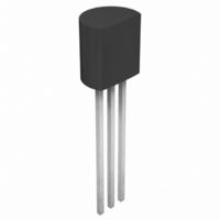
MCP1700-3002E/TO Microchip Technology, MCP1700-3002E/TO Datasheet - Page 5

MCP1700-3002E/TO
Manufacturer Part Number
MCP1700-3002E/TO
Description
IC REG LDO 250MA 3.0V TO-92-3
Manufacturer
Microchip Technology
Datasheet
1.SOT89-3EV-VREG.pdf
(24 pages)
Specifications of MCP1700-3002E/TO
Package / Case
TO-92-3 (Standard Body), TO-226
Regulator Topology
Positive Fixed
Voltage - Output
3V
Voltage - Input
Up to 6V
Voltage - Dropout (typical)
0.178V @ 250mA
Number Of Regulators
1
Current - Output
250mA (Min)
Operating Temperature
-40°C ~ 125°C
Mounting Type
Through Hole
Number Of Outputs
1
Polarity
Positive
Input Voltage Max
6 V
Output Voltage
3 V
Output Type
Fixed
Dropout Voltage (max)
350 mV
Output Current
250 mA
Line Regulation
0.75 % / V
Load Regulation
1 %
Voltage Regulation Accuracy
3 %
Maximum Power Dissipation
0.644 W
Maximum Operating Temperature
+ 125 C
Mounting Style
Through Hole
Minimum Operating Temperature
- 40 C
Primary Input Voltage
4V
Output Voltage Fixed
3V
Dropout Voltage Vdo
178mV
No. Of Pins
3
Voltage Regulator Case Style
TO-92
Operating Temperature Range
-40°C To +125°C
Rohs Compliant
Yes
Lead Free Status / RoHS Status
Lead free / RoHS Compliant
Current - Limit (min)
-
Lead Free Status / Rohs Status
Lead free / RoHS Compliant
Available stocks
Company
Part Number
Manufacturer
Quantity
Price
Part Number:
MCP1700-3002E/TO
Manufacturer:
MICROCHIP/微芯
Quantity:
20 000
2.0
Note: Unless otherwise indicated: V
T
Note: Junction Temperature (T
temperature. The test time is small enough such that the rise in Junction temperature over the Ambient temperature is not significant.
FIGURE 2-1:
Input Voltage.
FIGURE 2-2:
Current.
FIGURE 2-3:
Junction Temperature.
© 2007 Microchip Technology Inc.
A
Note:
= +25°C, V
50
45
40
35
30
25
20
15
10
3.0
2.8
2.6
2.4
2.2
2.0
1.8
1.6
1.4
1.2
1.0
2.50
2.25
2.00
1.75
1.50
1.25
5
0
0
2.0
TYPICAL PERFORMANCE CURVES
V
-40 -25 -10
R
V
I
OUT
= 2.8V
R
25
The graphs and tables provided following this note are a statistical summary based on a limited number of
samples and are provided for informational purposes only. The performance characteristics listed herein
are not tested or guaranteed. In some graphs or tables, the data presented may be outside the specified
operating range (e.g., outside specified power supply range) and therefore outside the warranted range.
= 1.2V
= 0 µA
2.5
IN
50
= V
V
R
3.0
T
= 5.0V
Junction Temperature (°C)
J
V
R
75
= +25°C
R
5
= 1.2V
+ V.
Input Voltage (V)
Load Current (mA)
Input Quiescent Current vs.
Ground Current vs. Load
Quiescent Current vs.
3.5
100
20
J
) is approximated by soaking the device under test to an ambient temperature equal to the desired junction
35
125
4.0
T
50
J
150
= +125°C
T
T
4.5
J
T
J
65
= +25°C
J
= +125°C
= - 40°C
R
V
175
R
= 1.8V, C
= 2.8V
80
5.0
V
200
I
OUT
IN
95
T
= V
J
= 0 µA
5.5
= - 40°C
225
R
110 125
+ 1V
OUT
6.0
250
= 1 µF Ceramic (X7R), C
FIGURE 2-4:
Voltage (V
FIGURE 2-5:
Voltage (V
FIGURE 2-6:
Voltage (V
1.206
1.204
1.202
1.200
1.198
1.196
1.194
1.192
1.190
1.795
1.785
1.775
2.800
2.798
2.796
2.794
2.792
2.790
2.788
2.786
2.784
2.782
2.780
2.778
1.79
1.78
1.77
1.8
3.3
2
2
R
R
R
T
IN
J
= 1.2V).
= 1.8V).
= 2.8V).
3.6
T
= - 40°C
2.5
2.5
J
= 1 µF Ceramic (X7R), I
= +125°C
T
T
J
J
= +125°C
= +25°C
3.9
T
J
3
3
= - 40°C
T
J
= - 40°C
Output Voltage vs. Input
Output Voltage vs. Input
Output Voltage vs. Input
4.2
Input Voltage (V)
Input Voltage (V)
Input Voltage (V)
3.5
3.5
T
J
4.5
= +25°C
MCP1700
4
4
4.8
T
J
4.5
4.5
= +25°C
T
5.1
J
= +125°C
DS21826B-page 5
L
5
5
V
I
V
I
V
I
OUT
5.4
OUT
OUT
R
R
R
= 100 µA,
= 2.8V
= 1.2V
= 1.8V
= 0.1 mA
= 0.1 mA
= 0.1 mA
5.5
5.5
5.7
6
6
6


