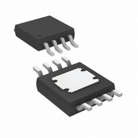
ADP125ARHZ-R7 Analog Devices Inc, ADP125ARHZ-R7 Datasheet - Page 12

ADP125ARHZ-R7
Manufacturer Part Number
ADP125ARHZ-R7
Description
IC REG LDO ADJ 500MA 8MSOP
Manufacturer
Analog Devices Inc
Specifications of ADP125ARHZ-R7
Regulator Topology
Positive Adjustable
Voltage - Output
0.8 ~ 5 V
Voltage - Input
2.3 ~ 5.5 V
Voltage - Dropout (typical)
0.13V @ 500mA
Number Of Regulators
1
Current - Output
500mA (Max)
Current - Limit (min)
550mA
Operating Temperature
-40°C ~ 85°C
Mounting Type
Surface Mount
Package / Case
8-MSOP Exposed Pad, 8-HMSOP, 8-eMSOP
Primary Input Voltage
5.5V
Output Voltage Adjustable Range
800mV To 5V
Dropout Voltage Vdo
130mV
No. Of Pins
8
Output Current
500mA
Voltage Regulator Case Style
MSOP
Operating Temperature Range
-40°C
Lead Free Status / RoHS Status
Lead free / RoHS Compliant
Other names
ADP125ARHZ-R7TR
ADP124/ADP125
APPLICATIONS INFORMATION
CAPACITOR SELECTION
Output Capacitor
The ADP124/ADP125 are designed for operation with small,
space-saving ceramic capacitors, but these devices can function
with most commonly used capacitors as long as care is taken to
ensure an appropriate effective series resistance (ESR) value. The
ESR of the output capacitor affects the stability of the LDO control
loop. A minimum of 0.70 µF capacitance with an ESR of 1 Ω or
less is recommended to ensure stability of the ADP124/ADP125.
The transient response to changes in load current is also affected by
the output capacitance. Using a larger value of output capacitance
improves the transient response of the ADP124/ADP125 to
dynamic changes in load current. Figure 30 and Figure 31 show
the transient responses for output capacitance values of 1 µF and
4.7 µF, respectively.
1
2
1
2
CH1
CH1
Figure 31. Output Transient Response, C
Figure 30. Output Transient Response, C
V
V
500mA Ω
V
V
500mA Ω
IN
OUT
IN
OUT
= 4V
= 4V
= 3.3V
= 3.3V
1mA TO 500mA LOAD STEP
1mA TO 500mA LOAD STEP
B
B
W
W
CH2 50.0mV
CH2 50.0mV
V
V
I
I
OUT
OUT
OUT
OUT
B
B
W
W
T
T
M400ns
M400ns
13.20%
13.60%
OUT
A CH1
A CH1
OUT
= 4.7 µF
= 1 µF
200mA
200mA
Rev. A | Page 12 of 20
Input Bypass Capacitor
Connecting a 1 µF capacitor from VIN to GND reduces the circuit
sensitivity to the printed circuit board (PCB) layout, especially
when a long input trace or high source impedance is encountered.
If greater than 1 µF of output capacitance is required, the input
capacitor should be increased to match it.
Input and Output Capacitor Properties
Any good quality ceramic capacitors can be used with the
ADP124/ADP125, as long as the capacitor meets the minimum
capacitance and maximum ESR requirements. Ceramic capacitors
are manufactured with a variety of dielectrics, each with different
behavior over temperature and applied voltage. Capacitors must
have an adequate dielectric to ensure the minimum capacitance
over the necessary temperature range and dc bias conditions.
Using an X5R or X7R dielectric with a voltage rating of 6.3 V or
10 V is recommended. However, using Y5V and Z5U dielectrics
are not recommended for any LDO, due to their poor temperature
and dc bias characteristics.
Figure 32 depicts the capacitance vs. capacitor voltage bias charac-
teristics of an 0402, 1 µF, 10 V X5R capacitor. The voltage stability
of a capacitor is strongly influenced by the capacitor size and the
voltage rating. In general, a capacitor in a larger package or of a
higher voltage rating exhibits better stability. The temperature
variation of the X5R dielectric is about ±15% over the −40°C to
+85°C temperature range and is not a function of package or
voltage rating.
Equation 1 can be used to determine the worst-case capacitance,
accounting for capacitor variation over temperature, component
tolerance, and voltage.
where:
C
C is the rated capacitance value.
TEMPCO is the worst-case capacitor temperature coefficient.
TOL is the worst-case component tolerance.
EFF
is the effective capacitance at the operating voltage.
C
Figure 32. Capacitance vs. Capacitor Voltage Bias Characteristics
EFF
1.10
1.05
1.00
0.95
0.90
0.85
0.80
0.75
0.70
= C × (1 − TEMPCO) × (1 − TOL)
0
1
2
BIAS VOLTAGE (V)
3
4
5
6
7
(1)


