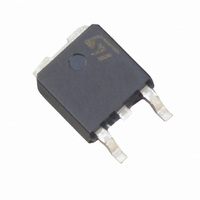
LD1117ADT-TR STMicroelectronics, LD1117ADT-TR Datasheet

LD1117ADT-TR
Specifications of LD1117ADT-TR
Available stocks
Related parts for LD1117ADT-TR
LD1117ADT-TR Summary of contents
Page 1
... Only chip trimming allows the regulator to reach a very tight output voltage tolerance, within ± °C. = 1.25 REF Order codes DPAK TO-220 LD1117ADT12TR LD1117ADT18TR LD1117ADT33TR LD1117AV33 LD1117ADT-TR Doc ID 7194 Rev 23 TO-220 SOT-223 DPAK Output voltage 1.2 V 1.8 V 3.3 V Adjustable from 1. 1/24 www.st.com ...
Page 2
Contents Contents 1 Diagram . . . . . . . . . . . . . . . . . . . . . . . . . . . . . . . . . . . . ...
Page 3
LD1117AXX12, LD1117AXX18, LD1117AXX33, LD1117AXX 1 Diagram Figure 1. Block diagram Doc ID 7194 Rev 23 Diagram 3/24 ...
Page 4
Pin configuration 2 Pin configuration Figure 2. Pin connections (top view) SOT-223 Note: The TAB is connected to the V 4/24 LD1117AXX12, LD1117AXX18, LD1117AXX33, LD1117AXX TO-220 . OUT Doc ID 7194 Rev 23 DPAK ...
Page 5
LD1117AXX12, LD1117AXX18, LD1117AXX33, LD1117AXX 3 Maximum ratings Table 2. Absolute maximum ratings Symbol V DC input voltage IN P Power dissipation D T Storage temperature range STG T Operating junction temperature range OP Note: Absolute maximum ratings are those values ...
Page 6
Schematic application 4 Schematic application Figure 3. Application circuit (for other fixed output voltages) 6/24 LD1117AXX12, LD1117AXX18, LD1117AXX33, LD1117AXX Doc ID 7194 Rev 23 ...
Page 7
LD1117AXX12, LD1117AXX18, LD1117AXX33, LD1117AXX 5 Electrical characteristics Refer to the test circuits, T GND, unless otherwise specified. Table 4. Electrical characteristics of LD1117A#12 Symbol Parameter V Output voltage O V Output voltage O ΔV Line regulation O ΔV Load regulation ...
Page 8
Electrical characteristics Refer to the test circuits, T specified. Table 5. Electrical characteristics of LD1117A#18 Symbol Parameter V Output voltage O V Output voltage O ΔV Line regulation O ΔV Load regulation O ΔV Temperature stability O ΔV Long term ...
Page 9
LD1117AXX12, LD1117AXX18, LD1117AXX33, LD1117AXX Refer to the test circuits, T specified. Table 6. Electrical characteristics of LD1117A#33 Symbol Parameter V Output voltage O V Output voltage O ΔV Line regulation O ΔV Load regulation O ΔV Temperature stability O ΔV ...
Page 10
Electrical characteristics Refer to the test circuits, T specified. Table 7. Electrical characteristics of LD1117A (Adjustable) Symbol Parameter V Output voltage O V Output voltage O ΔV Line regulation O ΔV Load regulation O ΔV Temperature stability O ΔV Long ...
Page 11
LD1117AXX12, LD1117AXX18, LD1117AXX33, LD1117AXX 6 Typical application Figure 4. Negative supply Figure 5. Active terminator for SCSI-2 bus Figure 6. Circuit for increasing output voltage Doc ID 7194 Rev 23 Typical application 11/24 ...
Page 12
Typical application Figure 7. Voltage regulator with reference Figure 8. Battery backed-up regulated supply 12/24 LD1117AXX12, LD1117AXX18, LD1117AXX33, LD1117AXX Doc ID 7194 Rev 23 ...
Page 13
LD1117AXX12, LD1117AXX18, LD1117AXX33, LD1117AXX Figure 9. Post-regulated dual supply Doc ID 7194 Rev 23 Typical application 13/24 ...
Page 14
LD1117A adjustable: application note LD1117AXX12, LD1117AXX18, LD1117AXX33, LD1117AXX 7 LD1117A adjustable: application note The LD1117A adjustable has a thermal stabilized 1.25 ± 0.012 V reference voltage between the OUT and ADJ pins normally fixed to 120 Ω. From ...
Page 15
LD1117AXX12, LD1117AXX18, LD1117AXX33, LD1117AXX 8 Package mechanical data In order to meet environmental requirements, ST offers these devices in different grades of ® ECOPACK packages, depending on their level of environmental compliance. ECOPACK specifications, grade definitions and product status are ...
Page 16
Package mechanical data Figure 12. Drawing dimension TO-220 (type STD-ST Dual Gauge) Note: 1 Maximum resin gate protrusion: 0.5 mm. 2 Resin gate position is accepted in each of the two positions shown on the drawing, or their symmetrical. 16/24 ...
Page 17
LD1117AXX12, LD1117AXX18, LD1117AXX33, LD1117AXX Figure 13. Drawing dimension TO-220 (type STD-ST Single Gauge) Doc ID 7194 Rev 23 Package mechanical data 8174627_B 17/24 ...
Page 18
Package mechanical data Figure 14. Drawing dimension tube for TO-220 Dual Gauge (mm.) Figure 15. Drawing dimension tube for TO-220 Single Gauge (mm.) 18/24 LD1117AXX12, LD1117AXX18, LD1117AXX33, LD1117AXX Doc ID 7194 Rev 23 ...
Page 19
LD1117AXX12, LD1117AXX18, LD1117AXX33, LD1117AXX Dim. Min 0.02 B 0.6 B1 2.9 c 0. 3.3 H 6.7 V SOT-223 mechanical data mm. Typ. Max. 1.8 0.1 0.7 0.85 3 3.15 0.26 0.35 6.5 6.7 ...
Page 20
Package mechanical data Dim. Min. A 2.2 A1 0.9 A2 0.03 B 0.64 b4 5.2 C 0. 4 (L1 0 0° 20/24 ...
Page 21
LD1117AXX12, LD1117AXX18, LD1117AXX33, LD1117AXX Tape & reel SOT223 mechanical data Dim. Min 12 6.73 Bo 7.32 Ko 1.78 Po 3.9 P 7.9 mm. Typ. Max. Min. 330 13.0 13.2 0.504 0.795 2.362 ...
Page 22
Package mechanical data Tape & reel DPAK-PPAK mechanical data Dim. Min 12 6.80 Bo 10.40 Ko 2.55 Po 3.9 P 7.9 22/24 LD1117AXX12, LD1117AXX18, LD1117AXX33, LD1117AXX mm. Typ. Max. 330 13.0 13.2 ...
Page 23
LD1117AXX12, LD1117AXX18, LD1117AXX33, LD1117AXX 9 Revision history Table 9. Document revision history Date Revision 29-Sep-2004 11 12-Oct-2004 12 21-Apr-2005 13 05-Jul-2005 14 10-Feb-2006 15 20-Dec-2006 16 19-Jan-2007 17 28-May-2007 18 07-Jun-2007 19 15-Apr-2008 20 28-Jul-2009 21 05-Jul-2010 22 16-Nov-2010 23 ...
Page 24
... Information in this document is provided solely in connection with ST products. STMicroelectronics NV and its subsidiaries (“ST”) reserve the right to make changes, corrections, modifications or improvements, to this document, and the products and services described herein at any time, without notice. All ST products are sold pursuant to ST’s terms and conditions of sale. ...


