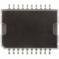
L4947PD STMicroelectronics, L4947PD Datasheet - Page 4

L4947PD
Manufacturer Part Number
L4947PD
Description
IC REG LDO W/RESET 20 PSOIC
Manufacturer
STMicroelectronics
Datasheet
1.L4947PD.pdf
(6 pages)
Specifications of L4947PD
Regulator Topology
Positive Fixed
Voltage - Output
5V
Voltage - Input
6 ~ 26 V
Voltage - Dropout (typical)
0.4V @ 500mA
Number Of Regulators
1
Current - Output
500mA
Operating Temperature
-40°C ~ 125°C
Mounting Type
Surface Mount
Package / Case
PowerSO-20 Exposed Bottom Pad
Lead Free Status / RoHS Status
Contains lead / RoHS non-compliant
Current - Limit (min)
-
Other names
497-1405-5
Available stocks
Company
Part Number
Manufacturer
Quantity
Price
Part Number:
L4947PD
Manufacturer:
ST
Quantity:
20 000
L4947PD
current) is maximum 13mA - over full T - when no
load current is required.
The internal antisaturation circuit allows a drastic
reduction in the current peak which takes place
during the start up.
The reset function supervises the regulator output
voltage inhibiting the microprocessor when the
device is out of regulation and resetting it at the
power-on after a settable delay. The reset is LOW
when the output voltage value is lower than the
reset threshold voltage. At the power-on phase
the output voltage increases (see Fig. 2) and -
when it reaches the power-on V
(On) - the reset output becomes HIGH after a de-
lay time set by the external capacitor C
power-off the output voltage decreases : at the
V
reset output instantaneously goes down (LOW
status) inhibiting the microprocessor. The typical
Figure 1: Typical Dropout Voltage vs. T
Figure 2: Reset Waveforms:
4/6
RT(Off)
threshold value (V
(I
(1) Without External Capacitor C
(2) With External Capacitor C
o
= 500mA).
V
V
RT(on)
RT(off
V
V
dthh
dthl
V
V
V
O
R
D
)
O
V rpeak
V rthys
-0.15V typ. value) the
O
threshold V
j
(1)
d
.
d
. At the
d
.
T d
(2)
RT
power on-off hysteresis is 50mV.
The three gain stages (operational amplifier,
driver and power PNP) require the external ca-
pacitor (C
stability of the system.
Load dump and field decay protections ( 80V),
reverse voltage (– 18V) and short circuit protec-
tion, thermal shutdown are the main features that
make the L4947PD specially suitable for applica-
tions in the automotive enviroment.
EXTERNAL COMPENSATION
Since the purpose of a voltage regulator is to sup-
ply and load variations, the open loop gain of the
regulator must be very high at low frequencies.
This may cause instability as a result of the vari-
ous poles present in the loop. To avoid this insta-
bility dominant pole compensation is used to re-
duce phase shift due to other poles at the unity
gain frequency. The lower the frequency of these
others poles at the unity gain frequency. The
lower the frequency of these other poles, the
greater must be capacitor esed to create the
dominant pole for the same DC gain.
Where the output transistor is a lateral PNP type
there is a pole in the regulation loop at a fre-
quencybtoo low to be compensated by a capaci-
tor which can be integrated. An external compen-
sation is therefore necessary so a very high value
capacitor must be connected from the output to
ground.
The paeassitic equivalent series resistance of the
capacitor used adds a zero to the regulation loop.
This zero may compromise the stability of the
system since its effect tends to cancel the effect
of the pole added. In regulators this ESR must be
less than 3
47 F.
(2)
omin
D94AT109
and the minimum capacitor value is
= 20 F) to guarantee the global
V disch
V rsat


