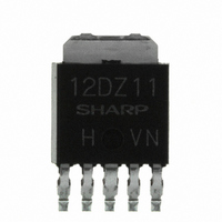
PQ12DZ11J00H Sharp Microelectronics, PQ12DZ11J00H Datasheet - Page 2

PQ12DZ11J00H
Manufacturer Part Number
PQ12DZ11J00H
Description
IC REG LDO 12V 1A ON/OFF SC-63
Manufacturer
Sharp Microelectronics
Datasheet
1.PQ3DZ13UJ00H.pdf
(9 pages)
Specifications of PQ12DZ11J00H
Regulator Topology
Positive Fixed
Voltage - Output
12V
Voltage - Input
Up to 24V
Voltage - Dropout (typical)
0.2V @ 500mA
Number Of Regulators
1
Current - Output
1A
Operating Temperature
-20°C ~ 80°C
Mounting Type
Surface Mount
Package / Case
SC-63
Lead Free Status / RoHS Status
Lead free / RoHS Compliant
Current - Limit (min)
-
Other names
425-2282-5
Fig.1 Test Circuit
Fig.3 Power Dissipation vs. Ambient
Electrical Characteristics
Note) Oblique line portion:Overheat protection may operate in this area.
V
7
4
5
6
7
8
9
Output voltage
Load regulation
Line regulation
Temperature coefficient of output voltage
Ripple Rejection
Dropout voltage
ON-state voltage for control
ON-state current for control
OFF-state voltage for control
OFF-state current for control
Quiescent current
Output OFF-state dissipation current
PQ3DZ53J000H/PQ3DZ13J000H: V
PQ3DZ53J000H/13J000H: V
Input voltage shall be the value when output voltage is 95% in comparison with the initial value. PQ3DZ53J000H/13J000H: V
In case of opening control terminal ② , output voltage turns off.
Applied only to PQ05DZ51J00H/11J00H.
PQ3DZ53J000H/PQ3DZ13J000H: ±0.02
I N
10
5
0
(Unless otherwise specified, condition shall be V
8
-20
Temperature
P
D
:With infinite heat sink
0.33μF
0
+
Ambient temperature T
20
Parameter
1
PQxxDZ51J00H series/PQ3DZ53J000H
PQxxDZ11J00H series/PQ3DZ13J000H
40
PQxxDZ51J00H series
PQxxDZ11J00H series
PQ3DZ53J000H/PQ3DZ13J000H
PQ05DZ51J00H
PQ09DZ51J00H
PQ12DZ51J00H
60
IN
A
5
=4 to 10V,PQ05DZ51J00H/11J00H: V
80
I q
IN
/
/
/
=5V,PQ05DZ51J00H/11J00H: V
100
3
2
PQ05DZ11J00H
PQ09DZ11J00H
PQ12DZ11J00H
Vc
A
a
120
(°C)
Ic
C
=2.7V,I
47μF
+
150
Symbol
O
V
=0.3A[PQxxDZ51J00H series/PQ3DZ53J000H], I
I
V
T
A
R
I
R
C(OFF)
RR
V
C(ON)
C(OFF)
I
V
I
C(ON)
C
qs
eg
q
eg
I-O
V
R
O
L
I
O
L
Vo
Io
V
I
I
Tj=0 to 125°C, I
Refer to Fig.2
I
V
I
V
IN
O
O
O
4
O
5
6
6
4
4
=6 to 16V,PQ09DZ51J00H/11J00H: V
IN
=5mA to 0.5A
=5mA to 1.0A
,I
,I
,I
C
C
=0A,
=0A,
=0.4V,I
=0.4V,I
=7V,PQ09DZ51J00H/11J00H: V
O
O
O
=5mA
=0.3A
=0.5A
2
4
4
O
O
=0A,
=0A,
Conditions
O
=5mA,
4
4
4
4
Fig.2 Test Circuit for Ripple Rejection
Fig.4 Overcurrent Protection Characteristics
e
V
12
10
11
4
9
8
7
6
5
4
3
2
1
0
i
IN
0
(Typical Value)
PQxxDZ51J00H Series/PQxxDZ11J00H Series
PQ3DZ53J000H/PQ3DZ13J000H
O
IN
=0.5A,[PQxxDZ11J00H series/PQ3DZ13J000H], ,
=11V,PQ12DZ51J00H/11J00H: V
V
0.33μF
IN
+
i-o
=10 to 20V,PQ12DZ51J00H/11J00H: V
=0.5V
Output current I
0.5
1
3.201
11.64
4.85
8.73
MIN.
2.0
45
-
-
-
-
-
-
-
-
-
IN
(PQ3DZ53J000H)
=3.7V
1.0
5
V
i-o
=1V
9
TYP.
12.0
8
8
3.3
5.0
9.0
8
±0.01
8
V
60
-
-
-
-
-
0.2
0.2
0.1
4
O
V
V
i-o
V
3
2
i-o
i-o
=5V
i-o
(A)
=2V
=3V
47μF
=10V
1.5
IN
2.7V
=14V
f=120Hz(sine wave)
ei(rms)=0.5V
VIN=5V(PQ3DZ53J000H/13J000H)
Io=0.3A
RR=20 log(ei(rms)/eo(rms))
3.399
12.36
MAX.
5.15
9.27
200
2.0
2.5
0.5
0.8
10
-
-
-
2
5
Sheet No.: OP06026
7V(PQ05DZ51J00H/11J00H)
11V(PQ09DZ51J00H/11J00H)
14V(PQ12DZ51J00H/11J00H)
IN
+
=13 to 23V
2.0
Io
4
%/°C
Ta=25˚C)
Unit
mA
dB
μA
μA
μA
%
%
V
V
V
V
+
R
L
V
e
o


