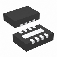
LT1965EDD#TRPBF Linear Technology, LT1965EDD#TRPBF Datasheet - Page 11

LT1965EDD#TRPBF
Manufacturer Part Number
LT1965EDD#TRPBF
Description
IC REG LDO 1.1A 8-DFN
Manufacturer
Linear Technology
Datasheet
1.LT1965EDD-3.3PBF.pdf
(20 pages)
Specifications of LT1965EDD#TRPBF
Regulator Topology
Positive Adjustable
Voltage - Output
1.2 ~ 19.5 V
Voltage - Input
1.8 ~ 20 V
Voltage - Dropout (typical)
0.31V @ 1.1A
Number Of Regulators
1
Current - Output
1.1A
Current - Limit (min)
1.2A
Operating Temperature
-40°C ~ 125°C
Mounting Type
Surface Mount
Package / Case
8-DFN
Lead Free Status / RoHS Status
Lead free / RoHS Compliant
Available stocks
Company
Part Number
Manufacturer
Quantity
Price
PIN FUNCTIONS
OUT (Pins 1, 2 / 1, 2 / 4 / 4): Output. This pin supplies
power to the load. Use a minimum output capacitor of
10μF to prevent oscillations. Large load transient applica-
tions require larger output capacitors to limit peak volt-
age transients. See the Applications Information section
for more information on output capacitance and reverse
output characteristics.
SENSE (Pin 3 / 3 / 5 / 5): Sense. For fi xed voltage ver-
sions of the LT1965 (LT1965-1.5/LT1965-1.8/ LT1965-2.5/
LT1965-3.3), the SENSE pin is the input to the error ampli-
fi er. Optimum regulation is obtained when the SENSE pin
is connected to the OUT pin of the regulator. In critical ap-
plications, small voltage drops are caused by the resistance
(R
These drops may be eliminated by connecting the SENSE
pin to the output at the load as shown in Figure 1 (Kelvin
Sense Connection). Note that the voltage drop across
the external PCB traces will add to the dropout voltage
of the regulator. The SENSE pin bias current is 100μA at
the nominal rated output voltage. The SENSE pin can be
pulled below ground (as in a dual supply system where
the regulator load is returned to a negative supply) while
still allowing the device to start and operate.
P
) of PCB traces between the regulator and the load.
V
IN
Figure 1. Kelvin Sense Connection
+
IN
SHDN
LT1965
GND
(DFN/MSOP/DD-PAK/TO-220)
SENSE
OUT
R
R
P
P
+
1965 F01
LOAD
ADJ (Pin 3 / 3 / 5 / 5): Adjust. This pin is the input to the
error amplifi er. It has a typical bias current of 1.3μA that
fl ows into the pin. The ADJ pin voltage is 1.20V referenced
to ground.
GND (Pins 4, 5 / 4, 5 / 3 / 3): Ground. For the adjustable
LT1965, connect the bottom of the resistor divider, setting
output voltage, directly to GND for optimum regulation.
SHDN (Pin 6 / 6 / 1 / 1): Shutdown. Pulling the SHDN
pin low puts the LT1965 into a low power state and turns
the output off. Drive the SHDN pin with either logic or an
open collector/drain with a pull-up resistor. The resistor
supplies the pull-up current to the open collector/drain
logic, normally several microamperes and the SHDN pin
current, typically less than 5.5μA. If unused, connect the
SHDN pin to V
GND unless it is tied to the IN pin. If the SHDN pin is
driven below GND while IN is powered, the output will
turn on. SHDN pin logic cannot be referenced to a nega-
tive supply rail.
IN (Pins 7, 8 / 7, 8 / 2 / 2): Input. This pin supplies power
to the device. The LT1965 requires a bypass capacitor at IN
if located more than six inches from the main input fi lter
capacitor. Include a bypass capacitor in battery-powered
circuits as a battery’s output impedance generally rises with
frequency. A bypass capacitor in the range of 1μF to 10μF
suffi ces. The LT1965’s design withstands reverse voltages
on the IN pin with respect to ground and the OUT pin. In
the case of a reversed input, which occurs if a battery is
plugged in backwards, the LT1965 behaves as if a diode
is in series with its input. No reverse current fl ows into
the LT1965 and no reverse voltage appears at the load.
The device protects itself and the load.
Exposed Pad (Pin 9 / 9, DFN and MSOP Packages Only):
Ground. Tie this pin directly to Pins 4 and 5 and the PCB
ground. This pin provides enhanced thermal performance
with its connection to the PCB ground. See the Applica-
tions Information section for thermal considerations and
calculating junction temperature.
IN
. The SHDN pin cannot be driven below
LT1965 Series
11
1965fa


