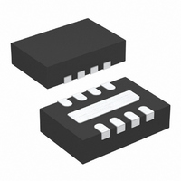
LT1965EDD#TRPBF Linear Technology, LT1965EDD#TRPBF Datasheet - Page 14

LT1965EDD#TRPBF
Manufacturer Part Number
LT1965EDD#TRPBF
Description
IC REG LDO 1.1A 8-DFN
Manufacturer
Linear Technology
Datasheet
1.LT1965EDD-3.3PBF.pdf
(20 pages)
Specifications of LT1965EDD#TRPBF
Regulator Topology
Positive Adjustable
Voltage - Output
1.2 ~ 19.5 V
Voltage - Input
1.8 ~ 20 V
Voltage - Dropout (typical)
0.31V @ 1.1A
Number Of Regulators
1
Current - Output
1.1A
Current - Limit (min)
1.2A
Operating Temperature
-40°C ~ 125°C
Mounting Type
Surface Mount
Package / Case
8-DFN
Lead Free Status / RoHS Status
Lead free / RoHS Compliant
Available stocks
Company
Part Number
Manufacturer
Quantity
Price
LT1965 Series
APPLICATIONS INFORMATION
recover. Other regulators, such as the LT1083/LT1084/
LT1085 family, also exhibit this phenomenon, so it is not
unique to the LT1965.
The problem occurs with a heavy output load when the
input voltage is high and the output voltage is low. Com-
mon situations occur immediately after the removal of a
short-circuit or if the shutdown pin is pulled high after the
input voltage has already been turned on. The load line for
such a load may intersect the output current curve at two
points. If this happens, there are two stable output operating
points for the regulator. With this double intersection, the
input power supply may need to be cycled down to zero
and brought up again to make the output recover.
Output Voltage Noise
The LT1965 regulators are designed to provide low output
voltage noise over the 10Hz to 100kHz bandwidth while
operating at full load. Output voltage noise is approximately
80nV/√Hz over this frequency bandwidth for the LT1965
adjustable version. For higher output voltages (generated
by using a resistor divider), the output voltage noise gains
up accordingly.
Higher values of output voltage noise may be measured
if care is not exercised with regard to circuit layout and
testing. Crosstalk from nearby traces can induce unwanted
noise onto the LT1965’s output. Power supply ripple rejec-
tion must also be considered; the LT1965 regulators do
not have unlimited power supply rejection and will pass a
small portion of the input noise through to the output.
14
Thermal Considerations
The LT1965’s maximum rated junction temperature of
125°C limits its power handling capability. Two compon-
ents comprise the power dissipated by the device:
1. Output current multiplied by the input/output voltage
2. GND pin current multiplied by the input voltage:
GND pin current is determined using the GND Pin Current
curves in the Typical Performance Characteristics section.
Power dissipation equals the sum of the two components
listed.
The LT1965 regulators have internal thermal limiting that
protect the device during overload conditions. For con-
tinuous normal conditions, do not exceed the maximum
junction temperature rating of 125°C. Carefully consider
all sources of thermal resistance from junction to ambi-
ent including other heat sources mounted in proximity to
the LT1965.
The underside of the LT1965 DFN package has exposed
metal (4mm
The underside of the LT1965 MSOP package also has
exposed metal (3.7mm
directly transfer from the die junction to the printed circuit
board metal to control maximum operating junction tem-
perature. The dual-in-line pin arrangement allows metal
to extend beyond the ends of the package on the topside
(component side) of a PCB. Connect this metal to GND
on the PCB. The multiple IN and OUT pins of the LT1965
also assist in spreading heat to the PCB.
For surface mount devices, heat sinking is accomplished
by using the heat spreading capabilities of the PC board
and its copper traces. Copper board stiffeners and plated
through-holes can also be used to spread the heat gener-
ated by power devices.
differential: I
I
GND
• V
IN
2
) from the lead frame to the die attachment.
OUT
• (V
IN
2
). Both packages allow heat to
– V
OUT
), and
1965fa


