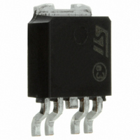
LD39150PT-R STMicroelectronics, LD39150PT-R Datasheet

LD39150PT-R
Specifications of LD39150PT-R
LD39150PT-R
Available stocks
Related parts for LD39150PT-R
LD39150PT-R Summary of contents
Page 1
... The device is developed on a BiCMOS process which allows low quiescent current operation independently of output load current. Order codes PPAK (T&R) LD39150PT18-R LD39150PT25-R LD39150PT33-R LD39150PT-R Rev 2 LD39150xx DPAK PPAK DFN6 (3x3 mm) Output voltages (1) DFN LD39150PU12R 1 ...
Page 2
Contents 1 Diagram . . . . . . . . . . . . . . . . . . . . . . . . . . . . . . . . . . . . . ...
Page 3
Diagram Figure 1. Block diagram (*) Not present on ADJ versions. 3/19 ...
Page 4
Pin configuration Figure 2. Pin connections (top view for DPAK and PPAK, bottom view for DFN) DFN6 (3x3 mm) Table 2. Pin description Pin n° SYMBOL DFN PPAK DPAK V /N.C. SENSE 5 5 ADJ ...
Page 5
Typical application circuits (C and C capacitors must be placed as close as possible to the IC pins Figure 3. LD39150xx fixed version with inhibit Note: Inhibit pin is not internally pulled down/up then it must not ...
Page 6
Figure 5. LD39150xx DPAK Figure 6. Timing diagram 6/19 ...
Page 7
Maximum ratings Table 3. Absolute maximum ratings Symbol V DC input voltage I V INHIBIT input voltage INH V DC output voltage O V ADJ pin voltage ADJ I Output current O P Power dissipation D T Storage temperature ...
Page 8
Electrical characteristics Table 5. Electrical characteristics ( ° specified) Symbol Parameter V Operating input voltage I V Output voltage tolerance O V Reference voltage REF Output voltage LINE ΔV O regulation ...
Page 9
Typical performance characteristics ( ° specified) Figure 7. Output voltage vs temperature Figure 9. Dropout voltage vs output current Figure 11. Quiescent current vs temperature + ...
Page 10
Figure 13. Short circuit current vs temperature Figure 14. Output voltage vs input voltage Figure 15. Stability region vs C kHz) Figure 17. Load transient V = 3.5V 10mA to 1.5A 1µ ...
Page 11
Application notes 7.1 External capacitors The LD39150xx requires external capacitors for regulator stability. These capacitors must be selected to meet the requirements of minimum capacitance and equivalent series resistance (see Figure 15 and from the relative pins and connected ...
Page 12
Package mechanical data In order to meet environmental requirements, ST offers these devices in different grades of ECOPACK® packages, depending on their level of environmental compliance. ECOPACK® specifications, grade definitions and product status are available at: ECOPACK® ...
Page 13
PPAK mechanical data mm. Dim. Min. Typ. A 2.2 A1 0.9 A2 0.03 B 0.4 B2 5.2 C 0. 5.1 E 6.4 E1 4.7 e 1.27 G 4.9 G1 2.38 H 9.35 L2 0.8 L4 ...
Page 14
Dim. Min. A 2.2 A1 0.9 A2 0.03 B 0.64 b4 5.2 C 0. 4 (L1 0 0° 14/19 DPAK mechanical data ...
Page 15
DFN6 (3x3 mm) mechanical data mm. Dim. Min. Typ. A 0.80 0. 0.02 A3 0.20 b 0.23 0.30 D 2.90 3.00 D2 2.23 2.38 E 2.90 3.00 E2 1.50 1.65 e 0.95 L 0.30 0.40 inch. Max. Min. ...
Page 16
Tape & reel DPAK-PPAK mechanical data Dim. Min 12 6.80 Bo 10.40 Ko 2.55 Po 3.9 P 7.9 16/19 mm. Typ. Max. Min. 330 13.0 13.2 0.504 0.795 2.362 22.4 6.90 7.00 ...
Page 17
Tape & reel QFNxx/DFNxx (3x3) mechanical data mm. Dim. Min. Typ 12 3.3 Bo 3 Max. Min. 180 13.2 0.504 0.795 2.362 14 inch. Typ. Max. ...
Page 18
Revision history Table 6. Document revision history Date Revision 26-Jan-2007 1 12-Jan-2009 2 18/19 Changes Initial release. Removed: package DFN8 (4x4 mm) and added package DFN6 (3x3 mm). ...
Page 19
... Information in this document is provided solely in connection with ST products. STMicroelectronics NV and its subsidiaries (“ST”) reserve the right to make changes, corrections, modifications or improvements, to this document, and the products and services described herein at any time, without notice. All ST products are sold pursuant to ST’s terms and conditions of sale. ...


