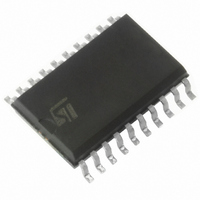
L4938ED013TR STMicroelectronics, L4938ED013TR Datasheet - Page 12

L4938ED013TR
Manufacturer Part Number
L4938ED013TR
Description
IC REG 5V/ADV DUAL LDO 20SOIC
Manufacturer
STMicroelectronics
Series
-r
Datasheet
1.L4938EPD13TR.pdf
(20 pages)
Specifications of L4938ED013TR
Regulator Topology
Positive Fixed and Adjustable
Voltage - Output
5V, 4.9 ~ 5.1 V
Voltage - Input
Up to 28V
Voltage - Dropout (typical)
0.2V @ 100mA, 0.3V @ 400mA
Number Of Regulators
2
Current - Output
100mA, 400mA
Current - Limit (min)
100mA, 450mA
Operating Temperature
-40°C ~ 150°C
Mounting Type
Surface Mount
Package / Case
20-SOIC (7.5mm Width)
Polarity
Positive
Number Of Outputs
2
Output Type
Fixed
Output Voltage
5 V
Output Current
5 mA
Line Regulation
20 mV
Load Regulation
50 mV
Dropout Voltage (max)
0.2 V
Input Voltage Max
20 V
Maximum Operating Temperature
+ 150 C
Minimum Operating Temperature
- 40 C
Maximum Power Dissipation
875 mW
Mounting Style
SMD/SMT
Reference Voltage
1.23 V
Voltage Regulation Accuracy
2 %
Lead Free Status / RoHS Status
Contains lead / RoHS non-compliant
Other names
497-3355-2
Available stocks
Company
Part Number
Manufacturer
Quantity
Price
Company:
Part Number:
L4938ED013TR
Manufacturer:
OKISEMICONDUCTOR
Quantity:
2 854
Part Number:
L4938ED013TR
Manufacturer:
ST
Quantity:
20 000
Application information
3.3
3.4
12/20
In the standby mode when the output 2 is disabled, the current consumption of the device
(quiescent current) is less than 90 µA (14 V supply voltage).
To reduce the quiescent current peak in the undervoltage region and to improve the
transient response in this region, the dropout voltage is controlled. A second regulation path
keeps the output voltage without load below 5.5 V even at high temperatures.
Output 2 voltage
The output 2 regulator uses the same output structure as the standby regulator but rated for
the output current of 400 mA. The output voltage is internally fixed to 5 V if ADJ is
connected to V
Figure 4.
Connecting a resistor divider R
programmed to the value of
with R
temperature coefficient (T
account. Pin ADJ in this mode should not have a capacitive burden because this would
reduce the phase margin of the regulator loop.
Reset circuit
The reset circuit supervises the standby output voltage. The reset output (RES) is defined
from V
V
The reset threshold of 4.7 V is defined with the internal reference voltage
output divider, when pin PR is left open. The reset threshold voltage can be programmed in
the range from 3.8 V to 4.7 V by connecting an external resistor from pin PR to GND.
OUT1
ADJ
.
OUT
= 60 K to 150 K and V
≥ 1 V. Even if V
OUT2
OUT2
. The output 2 regulator can be switches OFF via the enable input.
V
C
OUT2
S
- 2000 pprm) of the internal resistor (R
is lacking, the reset generator is supplied by the output voltage
Doc ID 17243 Rev 1
1E
OUT1
=
, R
V
2E
OUT1
= 4.95 to 5.05 V. For an exact calculation the
to the ADJ, OUT2 pin the output voltage 2 can be
⎛
⎜
⎝
1
+
R
------------------------------------------------ -
1E
R
(
2E
R
2E
⋅
R
+
ADJ
R
ADJ
)
⎞
⎟
⎠
ADJ
L4938ED, L4938EPD
) must be taken into
(a)
and standby


