LP38512MRX-ADJ/NOPB National Semiconductor, LP38512MRX-ADJ/NOPB Datasheet
LP38512MRX-ADJ/NOPB
Specifications of LP38512MRX-ADJ/NOPB
Available stocks


Related parts for LP38512MRX-ADJ/NOPB

LP38512MRX-ADJ/NOPB Summary of contents
Page 1
... LP38512-ADJ provides excellent transient performance to meet the demand of high performance digital core ASICs, DSPs, and FPGAs found in highly-intensive applications such as servers, routers/switches, and base stations. Typical Application Circuit © 2009 National Semiconductor Corporation LP38512-ADJ Features ■ 2.25V to 5.5V Input Voltage Range ■ ...
Page 2
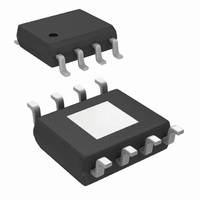
... Ordering Information Output Order Voltage Number LP38512MR-ADJ ADJ LP38512MRX-ADJ LP38512TJ-ADJ Connection Diagrams Top View TO-263 THIN 5-Pin Package Pin Descriptions for TO-263 THIN (TJ) Package Pin # Pin Name Function Enable. Pull high to enable the output, low to disable the output. This pin has no internal bias and ...
Page 3
... Absolute Maximum Ratings If Military/Aerospace specified devices are required, please contact the National Semiconductor Sales Office/ Distributors for availability and specifications. Storage Temperature Range Soldering Temperature (Note 3) Thin TO-263 PSOP-8 ESD Rating (Note 2) Power Dissipation (Note 4) Input Pin Voltage (Survival) Enable Pin Voltage (Survival) ...
Page 4
Symbol Parameter AC Parameters PSRR Ripple Rejection ρ Output Noise Density n(l/f) e Output Noise Voltage n Thermal Characteristics T Thermal Shutdown SD ΔT Thermal Shutdown Hysteresis T SD Thermal Resistance θ Junction to Ambient J-A (Note 4) Thermal Resistance ...
Page 5
Typical Performance Characteristics V = 2.0V µ µ OUT V vs Temperature ADJ Ground Pin Current (I GND Ground Pin Current ( Temperature GND Unless otherwise specified ...
Page 6
OUT Line Regulation vs Temperature Load Transient 1. μF Ceramic OUT ADJ OUT www.national.com EN 30040932 30040921 30040923 6 Load regulation vs Temperature 30040920 Current Limit vs ...
Page 7
Load Transient, 500 μF Ceramic V = 1.20V, C OUT OUT 30040925 Line Transient = 10 μF Ceramic V = 1.20V, C OUT OUT 30040927 PSRR 1.5A OUT = 10 μF Ceramic V ...
Page 8
Block Diagram Application Information EXTERNAL CAPACITORS Like any low-dropout regulator, external capacitors are re- quired to assure stability. These capacitors must be correctly selected for proper performance. Input Capacitor A ceramic input capacitor of at least 10 µF is required. ...
Page 9
Please refer to the POW- ER DISSIPATION/HEAT-SINKING section for power dissi- pation calculations. SETTING THE OUTPUT VOLTAGE The output voltage is set using the ...
Page 10
The maximum allowable junction temperature rise (ΔT pends on the maximum expected ambient temperature ( the application, and the maximum allowable junction (MAX) temperature (T ): J(MAX) Δ − J(MAX) A(MAX) The maximum allowable ...
Page 11
FIGURE 4. θ vs Thermal Via Count for the PSOP-8 JA Package on 2–Layer PCB with Copper Area on Bottom- Side Figure 5 shows thermal performance for a two layer board with the DAP soldered to copper area on the ...
Page 12
Physical Dimensions TO-263 THIN, 5 Lead, Molded, 1.7mm Pitch, Surface Mount www.national.com inches (millimeters) unless otherwise noted NS Package Number TJ5A PSOP, 8-Lead, Molded, 0.050in Pitch, Surface Mount NS Package Number MRA08A 12 ...
Page 13
Notes 13 www.national.com ...
Page 14
... For more National Semiconductor product information and proven design tools, visit the following Web sites at: Products Amplifiers www.national.com/amplifiers Audio www.national.com/audio Clock and Timing www.national.com/timing Data Converters www.national.com/adc Interface www.national.com/interface LVDS www.national.com/lvds Power Management www.national.com/power Switching Regulators www.national.com/switchers LDOs www.national.com/ldo LED Lighting www ...