NCP565D2TG ON Semiconductor, NCP565D2TG Datasheet - Page 2
NCP565D2TG
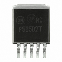
Manufacturer Part Number
NCP565D2TG
Description
IC REG LDO 1.5A ADJ VOLT D2PAK-5
Manufacturer
ON Semiconductor
Datasheet
1.NCP565V12EVB.pdf
(17 pages)
Specifications of NCP565D2TG
Regulator Topology
Positive Adjustable
Voltage - Output
0.9 ~ 7.7 V
Voltage - Input
2.5 ~ 9 V
Voltage - Dropout (typical)
0.9V @ 1.5A
Number Of Regulators
1
Current - Output
1.5A
Current - Limit (min)
1.6A
Operating Temperature
-40°C ~ 125°C
Mounting Type
Surface Mount
Package / Case
TO-263-5, D²Pak (5 leads + Tab), TO-263BA
Number Of Outputs
1
Polarity
Positive
Input Voltage Max
9 V
Output Voltage
0.9 V to 7.7 V
Output Type
Adjustable
Dropout Voltage (max)
1.3 V at 1500 mA
Output Current
1.5 A
Line Regulation
0.03 %
Load Regulation
0.03 %
Voltage Regulation Accuracy
3 %
Maximum Operating Temperature
+ 125 C
Mounting Style
SMD/SMT
Minimum Operating Temperature
- 40 C
Reference Voltage
0.927 V
Lead Free Status / RoHS Status
Lead free / RoHS Compliant
Other names
NCP565D2TG
NCP565D2TGOS
NCP565D2TGOS
Available stocks
Company
Part Number
Manufacturer
Quantity
Price


V
PIN DESCRIPTION
Adj. Version
in
Vin
D
Pin No.
3, Tab
Cin
2
PAK 5
1
2
4
5
Figure 1. Typical Application Schematic,
Reference
Voltage
Block
Figure 3. Block Diagram, Fixed Output
V
ref
Fixed Version
= 0.9 V
Vin
D
Pin No.
Shutdown
2, Tab
Thermal
2
PAK 3
Block
−
1
3
−
Fixed Output
NCP565
GND
GND
Output
Stage
Adj. Version
Vout
Pin No.
1, 2
3
6
4
5
DFN6
Current
Sense
Fixed Version
Limit
Cout
Pin No.
1, 2, 5
Vout
3
6
4
−
http://onsemi.com
Vout
Vin
Fixed Version
2
Cin
SOT−223
Pin No.
2, Tab
Vin
−
3
1
−
Figure 2. Typical Application Schematic,
Figure 4. Block Diagram, Adjustable Output
Reference
Voltage
Block
Vin
Symbol
Ground
V
N.C.
V
Adj
V
ref
Adjustable Output
out
in
NCP565
= 0.9 V
GND
Shutdown
Thermal
Block
−
Positive Power Supply Input Voltage
Power Supply Ground
Regulated Output Voltage
This pin is to be connected to the sense
resistors on the output. The linear
regulator will attempt to maintain 0.9 V
between this pin and ground. Refer to
the Application Information section for
output voltage setting.
Vout
ADJ
Output
Stage
GND
Description
5.6 pF
C1
Current
Sense
Limit
R1
R2
Cout
Vout
ADJ
Vout
Related parts for NCP565D2TG
Image
Part Number
Description
Manufacturer
Datasheet
Request
R

Part Number:
Description:
EVAL BOARD FOR NCP565V12
Manufacturer:
ON Semiconductor
Datasheet:

Part Number:
Description:
EVAL BOARD FOR NCP565VADJ
Manufacturer:
ON Semiconductor
Datasheet:

Part Number:
Description:
ON Semiconductor [VOLTAGE REGULATOR]
Manufacturer:
ON Semiconductor
Datasheet:
Part Number:
Description:
357-036-542-201 CARDEDGE 36POS DL .156 BLK LOPRO
Manufacturer:
ON Semiconductor
Datasheet:
Part Number:
Description:
357-036-542-201 CARDEDGE 36POS DL .156 BLK LOPRO
Manufacturer:
ON Semiconductor
Datasheet:
Part Number:
Description:
357-036-542-201 CARDEDGE 36POS DL .156 BLK LOPRO
Manufacturer:
ON Semiconductor
Datasheet:
Part Number:
Description:
357-036-542-201 CARDEDGE 36POS DL .156 BLK LOPRO
Manufacturer:
ON Semiconductor
Datasheet:
Part Number:
Description:
357-036-542-201 CARDEDGE 36POS DL .156 BLK LOPRO
Manufacturer:
ON Semiconductor
Datasheet:
Part Number:
Description:
357-036-542-201 CARDEDGE 36POS DL .156 BLK LOPRO
Manufacturer:
ON Semiconductor
Datasheet:
Part Number:
Description:
357-036-542-201 CARDEDGE 36POS DL .156 BLK LOPRO
Manufacturer:
ON Semiconductor
Datasheet:
Part Number:
Description:
357-036-542-201 CARDEDGE 36POS DL .156 BLK LOPRO
Manufacturer:
ON Semiconductor
Datasheet:
Part Number:
Description:
357-036-542-201 CARDEDGE 36POS DL .156 BLK LOPRO
Manufacturer:
ON Semiconductor
Datasheet:
Part Number:
Description:
357-036-542-201 CARDEDGE 36POS DL .156 BLK LOPRO
Manufacturer:
ON Semiconductor
Datasheet:
Part Number:
Description:
Manufacturer:
ON Semiconductor
Datasheet: