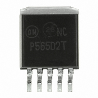
NCP565D2TG ON Semiconductor, NCP565D2TG Datasheet - Page 3

NCP565D2TG
Manufacturer Part Number
NCP565D2TG
Description
IC REG LDO 1.5A ADJ VOLT D2PAK-5
Manufacturer
ON Semiconductor
Datasheet
1.NCP565V12EVB.pdf
(17 pages)
Specifications of NCP565D2TG
Regulator Topology
Positive Adjustable
Voltage - Output
0.9 ~ 7.7 V
Voltage - Input
2.5 ~ 9 V
Voltage - Dropout (typical)
0.9V @ 1.5A
Number Of Regulators
1
Current - Output
1.5A
Current - Limit (min)
1.6A
Operating Temperature
-40°C ~ 125°C
Mounting Type
Surface Mount
Package / Case
TO-263-5, D²Pak (5 leads + Tab), TO-263BA
Number Of Outputs
1
Polarity
Positive
Input Voltage Max
9 V
Output Voltage
0.9 V to 7.7 V
Output Type
Adjustable
Dropout Voltage (max)
1.3 V at 1500 mA
Output Current
1.5 A
Line Regulation
0.03 %
Load Regulation
0.03 %
Voltage Regulation Accuracy
3 %
Maximum Operating Temperature
+ 125 C
Mounting Style
SMD/SMT
Minimum Operating Temperature
- 40 C
Reference Voltage
0.927 V
Lead Free Status / RoHS Status
Lead free / RoHS Compliant
Other names
NCP565D2TG
NCP565D2TGOS
NCP565D2TGOS
Available stocks
Company
Part Number
Manufacturer
Quantity
Price
Stresses exceeding Maximum Ratings may damage the device. Maximum Ratings are stress ratings only. Functional operation above the
Recommended Operating Conditions is not implied. Extended exposure to stresses above the Recommended Operating Conditions may affect
device reliability.
NOTE:
1. Refer to Electrical Characteristics and Application Information for Safe Operating Area.
2. As measured using a copper heat spreading area of 50 mm
3. Minimum V
ABSOLUTE MAXIMUM RATINGS
THERMAL CHARACTERISTICS
OPERATING RANGES
Input Voltage (Note 1)
Output Pin Voltage
Adjust Pin Voltage
Thermal Characteristics SOT−223 (Notes 1, 2)
Thermal Characteristics DFN6 (Notes 1, 2)
Thermal Characteristics D
Operating Input Voltage (Note 1)
Operating Junction Temperature Range
Operating Ambient Temperature Range
Storage Temperature Range
Thermal Resistance, Junction−to−Ambient
Thermal Resistance, Junction−to−Pin
Thermal Resistance, Junction−to−Ambient
Thermal Resistance, Junction−to−Pin
Thermal Resistance, Junction−to−Case
Thermal Resistance, Junction−to−Ambient
Thermal Resistance, Junction−to−Pin
This device series contains ESD protection and exceeds the following tests:
Human Body Model JESD 22−A114−B
Machine Model JESD 22−A115−A
in
= (V
out
+ V
2
DO
PAK (5ld) (Notes 1, 2)
) or 2.5 V, whichever is higher.
Rating
Rating
Rating
http://onsemi.com
2
, 1 oz copper thickness.
3
Symbol
Symbol
Symbol
R
R
R
R
R
R
R
V
V
T
V
V
T
T
out
adj
qJA
qJP
qJA
qJP
qJC
qJA
qJP
stg
in
in
A
J
2.5 (Note 3) to 9
−0.3 to V
−0.3 to V
V
−40 to 150
−40 to 125
−55 to 150
out
Value
Value
Value
107
176
105
+ V
18
12
37
3
4
in
in
DO
+ 0.3
+ 0.3
,
°C/W
°C/W
°C/W
Unit
Unit
Unit
°C
°C
°C
V
V
V
V


