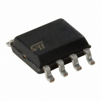
L9700D013TR STMicroelectronics, L9700D013TR Datasheet

L9700D013TR
Specifications of L9700D013TR
Available stocks
Related parts for L9700D013TR
L9700D013TR Summary of contents
Page 1
HIGH PERFORMANCE GROUND AND POSITIVE REFERENCE . VOLTAGE . FAST ACTIVE CLAMPING . OPERATING RANGE 4.75 - 5.25 V SINGLE VOLTAGE FOR SUPPLY AND POSITI REFERENCE . LOW QUIESCENT CURRENT LOW INPUT LEAKAGE CURRENT DESCRIPTION The ...
Page 2
L9700 ABSOLUTE MAXIMUM RATINGS Symbol V Supply Voltage CC I Input Current per Channel Junction and Storage Temperature j stg P Total Power Dissipation (T tot Note: The circuit is ESD protected according to MIL-STD-883C THERMAL ...
Page 3
Figure INPUT CHARACTERISTIC Limit Points of the Characteristic Approximation. Figure 2 : Dynamical Input Characteristics. 2a L9700 3/8 ...
Page 4
L9700 Figure 2 : Dynamical Input Characteristics (continued APPLICATION INFORMATION Most integrated circuits, both HNMOS and bipolar, are very sensitive to positive and negative overvol- tages on the supply and at the inputs. These transients occur in large ...
Page 5
Figure 3 : Typical Application. The minimum value for C is determined by the ac- IN curacy required, the time taken to sample the input and the input impedance during that time, while the maximum value is determined by the ...
Page 6
L9700 mm DIM. MIN. TYP. MAX. MIN. A 3.32 a1 0.51 0.020 B 1.15 1.65 0.045 b 0.356 0.55 0.014 b1 0.204 0.304 0.008 D 10.92 E 7.95 9.75 0.313 e 2.54 e3 7.62 e4 7.62 F 6.6 I 5.08 ...
Page 7
DIM. MIN. TYP. MAX. MIN. A 1.75 a1 0.1 0.25 0.004 a2 1.65 a3 0.65 0.85 0.026 b 0.35 0.48 0.014 b1 0.19 0.25 0.007 C 0.25 0.5 0.010 c1 45 (typ.) D (1) 4.8 5.0 0.189 E 5.8 ...
Page 8
... No license is granted by implication or otherwise under any patent or patent rights of STMicroelectronics. Specification mentioned in this publication are subject to change without notice. This publication supersedes and replaces all information previously supplied. STMi- croelectronics products are not authorized for use as critical components in life support devices or systems without express written approval of STMicroelectronics ...


