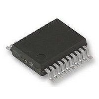
AD5781BRUZ Analog Devices Inc, AD5781BRUZ Datasheet - Page 21

AD5781BRUZ
Manufacturer Part Number
AD5781BRUZ
Description
IC DAC 18BIT SRL 20TSSOP
Manufacturer
Analog Devices Inc
Datasheet
1.AD5781ARUZ.pdf
(28 pages)
Specifications of AD5781BRUZ
Design Resources
18-Bit Accurate, low noise, precision bipolar DC voltage source (CN0177)
Settling Time
1µs
Number Of Bits
18
Data Interface
DSP, MICROWIRE™, QSPI™, Serial, SPI™
Number Of Converters
1
Voltage Supply Source
Analog and Digital, Dual ±
Operating Temperature
-40°C ~ 125°C
Mounting Type
Surface Mount
Package / Case
20-TSSOP
Resolution (bits)
18bit
Sampling Rate
1MSPS
Input Channel Type
Serial
Supply Current
600µA
Digital Ic Case Style
TSSOP
No. Of Pins
20
Operating Temperature Range
-40°C To +125°C
Supply Voltage Range - Analog
2.7V To 5.5V
Rohs Compliant
Yes
Lead Free Status / RoHS Status
Lead free / RoHS Compliant
Power Dissipation (max)
-
Lead Free Status / Rohs Status
Compliant
Available stocks
Company
Part Number
Manufacturer
Quantity
Price
Part Number:
AD5781BRUZ
Manufacturer:
ADI/亚德诺
Quantity:
20 000
Asynchronous DAC Update
In this mode, LDAC is held high while data is being clocked
into the input shift register. The DAC output is asynchronously
updated by taking LDAC low after SYNC has been taken high.
The update now occurs on the falling edge of LDAC .
Reset Function ( RESET )
The AD5781 can be reset to its power-on state by two means:
either by asserting the RESET pin or by utilizing the software
RESET control function (see
used, it should be hardwired to IOV
Table 9. Hardware Control Pins Truth Table
LDAC
X
X
0
0
1
1
0
1
0
1
ON-CHIP REGISTERS
DAC Register
Table 10 outlines how data is written to and read from the DAC register.
Table 10. DAC Register
MSB
DB23
R/W
R/W
1
The following equation describes the ideal transfer function of the DAC:
where:
V
V
D is the 18-bit code programmed to the DAC.
X is don’t care.
X is don’t care.
1
1
REFN
REFP
V
is the positive voltage applied at the V
is the negative voltage applied at the V
OUT
CLR
X
X
0
1
0
1
0
1
0
=
1
X
1
X
(
V
REFP
DB22
0
−
RESET
0
1
1
1
1
1
1
1
1
1
1
1
2
V
18
REFN
)
×
Table 14
D
Function
The AD5781 is in reset mode. The device cannot be programmed.
The AD5781 is returned to its power-on state. All registers are set to their default values.
The DAC register is loaded with the clearcode register value, and the output is set accordingly.
The output is set according to the DAC register value.
The DAC register is loaded with the clearcode register value, and the output is set accordingly.
The output is set according to the DAC register value.
The output remains at the clear code value.
The output remains set according to the DAC register value.
The output remains at the clear code value.
The DAC register is loaded with the clearcode register value and the output is set accordingly.
The DAC register is loaded with the clearcode register value and the output is set accordingly.
The output remains at the clear code value.
The output is set according to the DAC register value.
+
Register address
DB21
0
V
CC
REFN
). If the
.
REFPS
REFNS
RESET pin is not
input pin.
input pin.
DB20
1
Rev. 0 | Page 21 of 28
DB19
Asynchronous Clear Function (CLR)
The CLR pin is an active low clear that allows the output to be
cleared to a user defined value. The 18-bit clear code value is
programmed to the clearcode register (see
necessary to maintain
to complete the operation (see
is returned high, the output remains at the clear value (if LDAC
is high) until a new value is loaded to the DAC register. The
output cannot be updated with a new value while the CLR pin is
low. A clear operation can also be performed by setting the CLR
bit in the software control register (see
DAC register data
18-bits of data
DB2
CLR low for a minimum amount of time
Figure 2
DB1
X
Table 14
). When the
1
Table 13
).
). It is
CLR signal
AD5781
DB0
X
1
X
LSB


