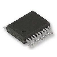
AD5781BRUZ Analog Devices Inc, AD5781BRUZ Datasheet - Page 22

AD5781BRUZ
Manufacturer Part Number
AD5781BRUZ
Description
IC DAC 18BIT SRL 20TSSOP
Manufacturer
Analog Devices Inc
Datasheet
1.AD5781ARUZ.pdf
(28 pages)
Specifications of AD5781BRUZ
Design Resources
18-Bit Accurate, low noise, precision bipolar DC voltage source (CN0177)
Settling Time
1µs
Number Of Bits
18
Data Interface
DSP, MICROWIRE™, QSPI™, Serial, SPI™
Number Of Converters
1
Voltage Supply Source
Analog and Digital, Dual ±
Operating Temperature
-40°C ~ 125°C
Mounting Type
Surface Mount
Package / Case
20-TSSOP
Resolution (bits)
18bit
Sampling Rate
1MSPS
Input Channel Type
Serial
Supply Current
600µA
Digital Ic Case Style
TSSOP
No. Of Pins
20
Operating Temperature Range
-40°C To +125°C
Supply Voltage Range - Analog
2.7V To 5.5V
Rohs Compliant
Yes
Lead Free Status / RoHS Status
Lead free / RoHS Compliant
Power Dissipation (max)
-
Lead Free Status / Rohs Status
Compliant
Available stocks
Company
Part Number
Manufacturer
Quantity
Price
Part Number:
AD5781BRUZ
Manufacturer:
ADI/亚德诺
Quantity:
20 000
AD5781
Control Register
The control register controls the mode of operation of the AD5781.
Table 11. Control Register
MSB
DB23
R/
R/
Table 12. Control Register Functions
Function
Reserved
RBUF
OPGND
DACTRI
BIN/2sC
SDODIS
LIN COMP
Clearcode Register
The clearcode register sets the value to which the DAC output is set when the CLR pin or CLR bit is asserted. The output value depends
on the DAC coding that is being used, either binary or twos complement. The default register value is 0.
Table 13. Clearcode Register
MSB
DB23
R/W
R/W
1
X is don’t care.
W
W
DB22
0
Register address
DB21
1
DB22
0
Output ground clamp control.
DAC register coding select.
Linearity error compensation for varying reference input spans. See the AD5781 Features section for further details.
Description
These bits are reserved and should be programmed to zero.
Output amplifier configuration control.
0: internal amplifier, A1, is powered up and resistors RFB and R1 are connected in series as shown in Figure 50. This allows
an external amplifier to be connected in a gain of two configurations. See the AD5781 Features section for further details.
1: (default) internal amplifier, A1, is powered down and resistors RFB and R1 are connected in parallel as shown in Figure 49
so that the resistance between the RFB and INV pins is 3.4 kΩ, equal to the resistance of the DAC. This allows the RFB and INV
pins to be used for input bias current compensation for an external unity gain amplifier. See the AD5781 Features section
for further details.
0: DAC output clamp to ground is removed, and the DAC is placed in normal mode.
1: (default) DAC output is clamped to ground through a ~6 kΩ resistance, and the DAC is placed in tristate mode.
DAC tristate control.
0: DAC is in normal operating mode.
1: (default) DAC is in tristate mode.
0: (default) DAC register uses twos complement coding.
1: DAC register uses offset binary coding.
SDO pin enable/disable control.
0: (default) SDO pin is enabled.
1: SDO pin is disabled (tristate).
0
1
0
1
DB20
0
0
0
Register address
DB21
1
Reserved
0
0
DB19...DB11
(Default) reference input span up to 10 V.
Reference input span of 20 V.
DB10
Reserved
DB20
1
DB9
LIN COMP
Rev. 0 | Page 22 of 28
DB19
DB8
DB7
Clearcode register data
Control register data
DB6
18-bits of data
DB5
SDODIS
DB2
DB4
BIN/2sC
DB3
DACTRI
DB2
OPGND
DB1
X
1
DB1
RBUF
DB0
X
1
DB0
Reserved
LSB
LSB


