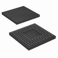
XR17V358IB176-F Exar Corporation, XR17V358IB176-F Datasheet - Page 20

XR17V358IB176-F
Manufacturer Part Number
XR17V358IB176-F
Description
IC UART PCIE OCTAL 176FPBGA
Manufacturer
Exar Corporation
Datasheet
1.XR17V358IB176-F.pdf
(68 pages)
Specifications of XR17V358IB176-F
Number Of Channels
1, UART
Package / Case
176-LFBGA
Features
*
Fifo's
256 Byte
Protocol
RS485
Voltage - Supply
1.2V, 3.3V
With Auto Flow Control
Yes
With Irda Encoder/decoder
Yes
With False Start Bit Detection
Yes
With Modem Control
Yes
Mounting Type
Surface Mount
Data Rate
25 Mbps
Supply Current
120 mA
Maximum Operating Temperature
+ 85 C
Minimum Operating Temperature
- 40 C
Mounting Style
SMD/SMT
Operating Supply Voltage
3.3 V
No. Of Channels
8
Uart Features
Tx/Rx FIFO Counters
Supply Voltage Range
3V To 3.6V
Operating Temperature Range
-40°C To +85°C
Digital Ic Case Style
BGA
No. Of Pins
176
Rohs Compliant
Yes
Lead Free Status / RoHS Status
Lead free / RoHS Compliant
For Use With
1016-1296 - EVAL BOARD FOR XR17V358-E81016-1295 - EVAL BOARD FOR XR17V358-E41016-1293 - EVAL BOARD FOR XR17V358
Lead Free Status / Rohs Status
Lead free / RoHS Compliant
Other names
1016-1294
Available stocks
Company
Part Number
Manufacturer
Quantity
Price
Company:
Part Number:
XR17V358IB176-F
Manufacturer:
EXAR
Quantity:
1 700
Company:
Part Number:
XR17V358IB176-F
Manufacturer:
Exar Corporation
Quantity:
10 000
Part Number:
XR17V358IB176-F
Manufacturer:
EXAR/艾科嘉
Quantity:
20 000
XR17V358
HIGH PERFORMANCE OCTAL PCI EXPRESS UART
Each bit gives an indication of the channel that has requested for service. Bit [0] represents channel 0 and
bit [7] indicates channel 7. Logic 1 indicates the channel N [7:0] has called for service. The interrupt bit clears
after reading the appropriate register of the interrupting channel register, see Interrupt Clearing section.
INT3, INT2 and INT1 [31:8] 3-bit Channel Interrupt Encoding
Each channel’s interrupt is encoded into 3 bits for receive, transmit, and status. Bits [10:8] represent channel 0
and go up to channel 7 with bits [31:29]. The 3-bit encoding and their priority order are shown below in
The wake-up interrupt, timer/counter interrupt and MPIO interrupt are only reported in channel 0 of INT1
(bits[10:8]). These interrupts are not reported in any other location.
F
P
IGURE
RIORITY
N+2
Bit
1
2
3
4
5
6
7
x
Channel-7
N+1
4. T
Bit
B
Bit
HE
N
IT
[
0
0
0
0
1
1
1
1
N
INT3 Register
G
N+2
+2]
Bit
LOBAL
Channel-6
N+1
Bit
B
IT
I
T
[
Bit
NTERRUPT
N
0
0
1
1
0
0
1
1
N
ABLE
+1]
The INT0 register provides individual status for each channel
N+2
Bit
Channel-5
7: UART C
Bit-7 Bit-6 Bit-5 Bit-4 Bit-3 Bit-2 Bit-1 Bit-0
N+1
Ch-7
Bit
B
IT
0
1
0
1
0
1
0
1
R
[
Individual UART Channel Interrupt Status
N
EGISTER
Bit
N
]
Ch-6
N+2
Bit
None or wake-up indicator (wake-up indicator is reported in channel 0 only)
RXRDY and RX Line Status (logic OR of LSR[4:1])
RXRDY Time-out
TXRDY, THR or TSR (auto RS485 mode) empty
MSR, RTS/CTS or DTR/DSR delta or Xoff/Xon det. or special char. detected
Reserved.
MPIO pin(s). Reported in channel 0 only.
Timer/Counter. Reported in channel 0 only.
HANNEL
Channel-4
Ch-5 Ch-4 Ch-3 Ch-2 Ch-1 Ch-0
INT0, INT1, INT2 and INT3
, INT0, INT1, INT2
N+1
Bit
Interrupt Registers,
INT2 Register
INT0 Register
Bit
N
[7:0] I
N+2
Bit
20
Channel-3
NTERRUPT
N+1
Bit
Bit
N
AND
N+2
I
Bit
NTERRUPT
S
Channel-2
INT3
OURCE
Ch-7 Ch-6 Ch-5 Ch-4
N+1
Bit-7
Bit
Bit-6
Bit
N
E
S
NCODING
OURCE
Bit-5
N+2
Bit
Channel-1
INT0 Register
Bit-4
N+1
INT1 Register
Bit
(
S
)
Ch-3 Ch-2 Ch-1 Ch-0
Bit-3
Bit
N
N+2
Bit-2
Bit
Channel-0
N+1
Bit-1
Bit
Bit-0
Bit
N
REV. 1.0.2
Table
7.


