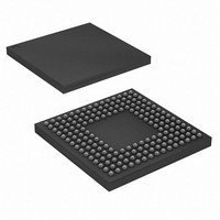
XR17V358IB176-F Exar Corporation, XR17V358IB176-F Datasheet - Page 52

XR17V358IB176-F
Manufacturer Part Number
XR17V358IB176-F
Description
IC UART PCIE OCTAL 176FPBGA
Manufacturer
Exar Corporation
Datasheet
1.XR17V358IB176-F.pdf
(68 pages)
Specifications of XR17V358IB176-F
Number Of Channels
1, UART
Package / Case
176-LFBGA
Features
*
Fifo's
256 Byte
Protocol
RS485
Voltage - Supply
1.2V, 3.3V
With Auto Flow Control
Yes
With Irda Encoder/decoder
Yes
With False Start Bit Detection
Yes
With Modem Control
Yes
Mounting Type
Surface Mount
Data Rate
25 Mbps
Supply Current
120 mA
Maximum Operating Temperature
+ 85 C
Minimum Operating Temperature
- 40 C
Mounting Style
SMD/SMT
Operating Supply Voltage
3.3 V
No. Of Channels
8
Uart Features
Tx/Rx FIFO Counters
Supply Voltage Range
3V To 3.6V
Operating Temperature Range
-40°C To +85°C
Digital Ic Case Style
BGA
No. Of Pins
176
Rohs Compliant
Yes
Lead Free Status / RoHS Status
Lead free / RoHS Compliant
For Use With
1016-1296 - EVAL BOARD FOR XR17V358-E81016-1295 - EVAL BOARD FOR XR17V358-E41016-1293 - EVAL BOARD FOR XR17V358
Lead Free Status / Rohs Status
Lead free / RoHS Compliant
Other names
1016-1294
Available stocks
Company
Part Number
Manufacturer
Quantity
Price
Company:
Part Number:
XR17V358IB176-F
Manufacturer:
EXAR
Quantity:
1 700
Company:
Part Number:
XR17V358IB176-F
Manufacturer:
Exar Corporation
Quantity:
10 000
Part Number:
XR17V358IB176-F
Manufacturer:
EXAR/艾科嘉
Quantity:
20 000
XR17V358
HIGH PERFORMANCE OCTAL PCI EXPRESS UART
FCR[3]: DMA Mode Select
This bit has no effect since TXRDY and RXRDY pins are not available in this device. It is provided for legacy
software compatibility.
•
•
FCR[2]: TX FIFO Reset
This bit is only active when FCR bit [0] is active.
•
•
FCR[1]: RX FIFO Reset
This bit is only active when FCR bit [0] is active.
•
•
FCR[0]: TX and RX FIFO Enable
•
•
Logic 0 = Set DMA to mode 0 (default).
Logic 1 = Set DMA to mode 1.
Logic 0= No transmit FIFO reset (default).
Logic 1 = Reset the transmit FIFO pointers and FIFO level counter logic (the transmit shift register is not
cleared or altered). This bit will return to a logic 0 after resetting the FIFO.
Logic 0 = No receive FIFO reset (default).
Logic 1 = Reset the receive FIFO pointers and FIFO level counter logic (the receive shift register is not
cleared or altered). This bit will return to a logic 0 after resetting the FIFO.
Logic 0 = Disable the transmit and receive FIFO (default).
Logic 1 = Enable the transmit and receive FIFOs. This bit must be set to logic 1 when other FCR bits are
written or they will not be programmed.
T
Table-A
Table-B
T
RIGGER
ABLE
BIT [7]
FCTR
0
0
T
ABLE
BIT [6]
FCTR
16: T
0
1
RANSMIT AND
BIT [7]
FCR
0
0
1
1
0
0
1
1
BIT [6]
FCR
0
1
0
1
0
1
0
1
R
ECEIVE
BIT [5]
FCR
0
0
0
1
1
FIFO T
BIT [4]
52
FCR
0
0
1
0
1
RIGGER
T
RIGGER
1 (default)
R
T
ABLE AND
ECEIVE
14
16
24
28
4
8
8
L
EVEL
L
EVEL
1 (default)
T
T
RANSMIT
RIGGER
L
EVEL
16
24
30
8
S
ELECTION
16C550, 16C2550,
16C2552, 16C554,
16C580, 16L580
16C650A, 16L651
C
OMPATIBILITY
REV. 1.0.2


