EVAL6229QR STMicroelectronics, EVAL6229QR Datasheet - Page 6
EVAL6229QR
Manufacturer Part Number
EVAL6229QR
Description
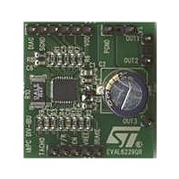
BOARD DEMO L6229Q BLDC MOT CTRL
Manufacturer
STMicroelectronics
Type
Motor / Motion Controllers & Driversr
Specifications of EVAL6229QR
Main Purpose
Power Management, Motor Control
Embedded
No
Utilized Ic / Part
L6229Q
Primary Attributes
3-Ph BLDC, 8 ~ 52V Output, PWM Current Control, Brake Function
Secondary Attributes
Over Current, Cross Conduction & Temperature Protection
Maximum Operating Temperature
+ 125 C
Operating Supply Voltage
8 V to 52 V
Product
Power Management Development Tools
Lead Free Status / RoHS Status
Lead free / RoHS Compliant
For Use With/related Products
L6229Q
Other names
497-10748


Demonstration board description
6/10
Table 3.
The input lines EN, BRAKE and F/R are connected to ground through a pull-down resistor
which sets the default logic level to “low”. An external signal can be applied to change each
input status. The Hall effect inputs H1, H2 and H3 have a pull-up resistor connected to the
V
A charge pump circuit, made up of D1, C3 and C4, generates the supply voltage for the
high-side integrated MOSFETs. Due to voltage and current switching at relatively high
frequency, these components are connected through short paths in order to minimize
induced noise in other circuits.
R4 and C5 are used by the integrated overcurrent protection circuitry to set the protection
timings (disable time t
the values in
R8 and C6 are used to set the off-time t
RC network value, the off-time should be adjusted according to the electrical characteristics
and supply voltage of the motor.
R11, R12 and C8 are low-pass filters to provide an external reference voltage through the
PWM output of a microcontroller.
R9 and C7 are used to set the off-time t
can be used to implement a simple frequency-to-voltage converter (speed loop control).
Figure
the EVAL6229QR demonstration board. A GND area is used for the IC power dissipation.
DD
R1, R2, R3, R4
Part reference
R5, R6, R7
voltage, which can be provided by the VDD pin.
C4, C8
4,
R10
R11
R12
C1
C2
C3
C5
C6
C7
D1
R8
R9
U1
Figure 5
EVAL6229QR component list
Table
and
3).
DISABLE
100kΩ 5% 0.25W
100kΩ 1% 0.25W
Figure 6
10kΩ 5% 0.25W
20kΩ 1% 0.25W
20kΩ 5% 0.25W
2kΩ 5% 0.25W
220nF/100V
100µF/63V
220nF/25V
Part value
BAT46SW
10nF/25V
0.4Ω 1W
L6229Q
820pF
5.6nF
10nF
is about 200 µs and delay time t
Doc ID 16960 Rev 1
show the component placement and the two-layer layout of
OFF
PULSE
of the PWM to about 50 µs. When changing the
of the TACHO pin. The TACHO output signal
3-phase BLDC motor driver in VFQFPN5x5
Part description
DELAY
Capacitor
Capacitor
Capacitor
Capacitor
Capacitor
Capacitor
Resistor
Resistor
Resistor
Resistor
Resistor
Resistor
Resistor
Resistor
Diodes
is about 1 µs, based on
AN3134
Related parts for EVAL6229QR
Image
Part Number
Description
Manufacturer
Datasheet
Request
R

Part Number:
Description:
ENERCHIP CC EVAL KIT
Manufacturer:
Cymbet Corporation
Datasheet:

Part Number:
Description:
BOARD EVAL FOR AD976
Manufacturer:
Analog Devices Inc
Datasheet:

Part Number:
Description:
BOARD EVAL FOR ADXL345
Manufacturer:
Analog Devices Inc
Datasheet:

Part Number:
Description:
ENERCHIP CC SEH EVAL KIT
Manufacturer:
Cymbet Corporation
Datasheet:

Part Number:
Description:
ENERCHIP EP ENERGY HARVEST EVAL
Manufacturer:
Cymbet Corporation
Datasheet:

Part Number:
Description:
EVAL BOARD FOR TW6864-LB2-GR
Manufacturer:
Intersil
Datasheet:
Part Number:
Description:
EVAL BOARD FOR TW8816-LB3-GR
Manufacturer:
Intersil
Datasheet:
Part Number:
Description:
EVAL BOARD FOR TW8817-TA3-GRS
Manufacturer:
Intersil
Datasheet:

Part Number:
Description:
EVALUATION MODULE FOR ADUM4160
Manufacturer:
Analog Devices Inc
Datasheet:

Part Number:
Description:
BOARD EVALUATION ADCMP581BCP
Manufacturer:
Analog Devices Inc
Datasheet:
Part Number:
Description:
BOARD EVALUATION ADM1041
Manufacturer:
Analog Devices Inc
Datasheet:

Part Number:
Description:
EVAL BOARD FOR STM32F107VCT
Manufacturer:
STMicroelectronics
Datasheet:
Part Number:
Description:
BOARD EVAL FOR AD1954
Manufacturer:
Analog Devices Inc
Datasheet:
Part Number:
Description:
BOARD EVAL FOR AD1955
Manufacturer:
Analog Devices Inc
Datasheet:

Part Number:
Description:
BOARD EVAL FOR AD7655
Manufacturer:
Analog Devices Inc
Datasheet: