MGA-71543-BLKG Avago Technologies US Inc., MGA-71543-BLKG Datasheet - Page 15
MGA-71543-BLKG
Manufacturer Part Number
MGA-71543-BLKG
Description
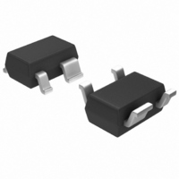
IC AMP MMIC LNA GAAS 3V SOT-343
Manufacturer
Avago Technologies US Inc.
Type
General Purpose Amplifierr
Datasheet
1.MGA-71543-BLKG.pdf
(24 pages)
Specifications of MGA-71543-BLKG
P1db
13.1dBm
Noise Figure
1.1dB ~ 1.45dB
Package / Case
SC-70-4, SC-82-4, SOT-323-4, SOT-343
Current - Supply
50mA ~ 60mA
Frequency
100MHz ~ 6GHz
Gain
14.4dB ~ 17.4dB
Rf Type
CDMA, TDMA, W-CDMA
Test Frequency
2.01GHz
Voltage - Supply
2.7V ~ 4.2V
Mounting Style
SMD/SMT
Technology
Low Noise Amplifier
Number Of Channels
1
Operating Frequency
6000 MHz
Operating Supply Voltage
3 V
Supply Current
50 mA
Maximum Power Dissipation
200 mW
Maximum Operating Temperature
+ 150 C
Manufacturer's Type
Low Noise Amplifier
Frequency (max)
6GHz
Operating Supply Voltage (min)
2.7V
Operating Supply Voltage (typ)
3V
Operating Supply Voltage (max)
4.2V
Package Type
SOT-343
Mounting
Surface Mount
Pin Count
3 +Tab
Noise Figure (typ)
1.1@6000MHzdB
Lead Free Status / RoHS Status
Lead free / RoHS Compliant
Lead Free Status / RoHS Status
Lead free / RoHS Compliant, Lead free / RoHS Compliant
Other names
516-1952
MGA-71543-BLKG
MGA-71543-BLKG
Available stocks
Company
Part Number
Manufacturer
Quantity
Price
Company:

Part Number:
MGA-71543-BLKG
Manufacturer:
NXP
Quantity:
12 000
Part Number:
MGA-71543-BLKG
Manufacturer:
AVAGO/安华高
Quantity:
20 000


15
Figure 4. Gate Bias Method.
The DC supply at the input
terminal (V
through a RF choke (inductor).
The voltage at V
respect to ground determines the
device current, I
I
Maximum device current
(approximately 60 mA) occurs at
V
When using the gate biasing
method, the bypass mode is
activated when V
V
Figure 5. Device Current vs. V
This kind of biasing would not
usually be used unless a negative
supply voltage was readily
available.
Source Resistor Bias
This is the recommended method
because it only requires one
(positive) power supply. As shown
in Figure 6, Pin 3 is DC grounded
and pins 1 and 4 are RF bypassed.
V
d
Input
ref
ref
ref
vs. V
70
60
50
40
30
20
10
= 0 (i.e. V
< -2V.
0
-1
ref
is shown in Figure 5.
4
3
ref
-0.8
) can be applied
gs
= 0).
ref
d
V
ds
. A plot of typical
ref
-0.6
2
1
(Pin 3) with
= 0V and
(V)
ref
Output
& V d
.
-0.4
-0.2
The current of the amplifier (I
set by the value of the resistor
R
connected at Pin 4 as shown in
Figure 6 and RF bypassed. At least
two capacitors in parallel are
recommended for RF bypassing.
One capacitor (100 pF) for high
frequency bypassing and a second,
large value capacitor for better
low frequency bypassing. The
large value capacitor is added in
parallel to improve the IP3
because they help ground the low
frequency mixing terms that are
generated during a two tones test
(i.e. f
separation of the two tones
usually 1 to a few MHz) and thus
improve the IIP3.
Figure 6. Source Resistor Bias Method.
Maximum current (about 60 mA)
occurs when R
A plot of typical I
shown in Figure 7.
Figure 7. Device Current vs. R
Input
bias
60
50
40
30
20
10
0
. This resistor (R
0
1
– f
R bias
20
2
3
4
term which is the
40
bias
60
R
bias
d
2
1
= 0.
vs. R
(Ω)
80
bias
Output
bias
& V d
bias
100
) is
.
is
120
d
) is
140
The approximate value of the
external resistor, R
be calculated from:
where R
desired device current in mA.
A simple method for DC ground-
ing the input terminal (Pin 3) is to
use a shunt inductor that is also
part of the noise-matching
network.
Adaptive Biasing
For applications in which input
power levels vary over a wide
range, it may be useful to dynami-
cally adapt the bias of the
MGA-71543 to match the signal
level. A sensor senses the signal
level at some point in the system
(usually in the baseband circuitry)
and automatically adjusts the bias
current of the amplifier accord-
ingly. The main advantage of
adaptive biasing is conservation of
supply current (longer battery life)
by using only the amount of
current necessary to handle the
input signal without distortion.
Adaptive biasing of the
MGA-71543 can be accomplished
by simple digital means (Figure 8).
For instance simple electronic
switches can be used to control
the value of the source resistor in
discrete increment.
Figure 8. Adaptive Bias Control using Digital
Method.
R
bias
DC
Return
Path
bias
3
= 964 (1 – 0.112
is in ohms and I
1
I
d
4
bias
2
, may also
Control
Digital
√
d
I
d
is the
)
Related parts for MGA-71543-BLKG
Image
Part Number
Description
Manufacturer
Datasheet
Request
R

Part Number:
Description:
Amplifier IC
Manufacturer:
Avago Technologies US Inc.
Datasheet:

Part Number:
Description:
IC AMP MMIC LNA GAAS 3V SOT-343
Manufacturer:
Avago Technologies US Inc.
Datasheet:

Part Number:
Description:
AMPLIFIER RFIC GAAS, LOW NOISE
Manufacturer:
Avago Technologies US Inc.
Part Number:
Description:
IC,Microwave/Millimeter Wave Amplifier,SINGLE,GAAS,SOT-343R,PLASTIC
Manufacturer:
Avago Technologies US Inc.
Part Number:
Description:
IC,Microwave/Millimeter Wave Amplifier,SINGLE,GAAS,SOT-343R,PLASTIC
Manufacturer:
Avago Technologies US Inc.
Datasheet:

Part Number:
Description:
OPTOCOUPLER GATE DRV 2A 16-SOIC
Manufacturer:
Avago Technologies US Inc.
Datasheet:
Part Number:
Description:
OPTOCOUPLER 2CH 2.5A 16-SOIC
Manufacturer:
Avago Technologies US Inc.
Datasheet:

Part Number:
Description:
OPTOCOUPLER GATE DRV 0.4A 16SOIC
Manufacturer:
Avago Technologies US Inc.
Datasheet:

Part Number:
Description:
OPTOCOUPLER 2.0A 250KHZ 8-DIP
Manufacturer:
Avago Technologies US Inc.
Datasheet:

Part Number:
Description:
OPTOCOUPLER 2.0A 250KHZ GW 8-SMD
Manufacturer:
Avago Technologies US Inc.
Datasheet:

Part Number:
Description:
OPTOCOUPLER 2CH 15MBD 3.3V 8SOIC
Manufacturer:
Avago Technologies US Inc.
Datasheet:
Part Number:
Description:
OPTOCOUPLER DARL-OUT 8-DIP
Manufacturer:
Avago Technologies US Inc.
Datasheet:
Part Number:
Description:
OPTOCOUPLER IGBT DRIVE 0.4A 8DIP
Manufacturer:
Avago Technologies US Inc.
Datasheet:
Part Number:
Description:
OPTOCOUPLER DARL-OUT 8-DIP
Manufacturer:
Avago Technologies US Inc.
Datasheet:

Part Number:
Description:
OPTOCOUPLER 1CH 1MBS 8-SMD GW
Manufacturer:
Avago Technologies US Inc.
Datasheet: