MGA-71543-BLKG Avago Technologies US Inc., MGA-71543-BLKG Datasheet - Page 3
MGA-71543-BLKG
Manufacturer Part Number
MGA-71543-BLKG
Description
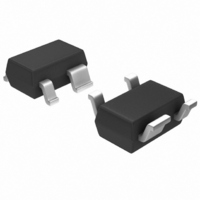
IC AMP MMIC LNA GAAS 3V SOT-343
Manufacturer
Avago Technologies US Inc.
Type
General Purpose Amplifierr
Datasheet
1.MGA-71543-BLKG.pdf
(24 pages)
Specifications of MGA-71543-BLKG
P1db
13.1dBm
Noise Figure
1.1dB ~ 1.45dB
Package / Case
SC-70-4, SC-82-4, SOT-323-4, SOT-343
Current - Supply
50mA ~ 60mA
Frequency
100MHz ~ 6GHz
Gain
14.4dB ~ 17.4dB
Rf Type
CDMA, TDMA, W-CDMA
Test Frequency
2.01GHz
Voltage - Supply
2.7V ~ 4.2V
Mounting Style
SMD/SMT
Technology
Low Noise Amplifier
Number Of Channels
1
Operating Frequency
6000 MHz
Operating Supply Voltage
3 V
Supply Current
50 mA
Maximum Power Dissipation
200 mW
Maximum Operating Temperature
+ 150 C
Manufacturer's Type
Low Noise Amplifier
Frequency (max)
6GHz
Operating Supply Voltage (min)
2.7V
Operating Supply Voltage (typ)
3V
Operating Supply Voltage (max)
4.2V
Package Type
SOT-343
Mounting
Surface Mount
Pin Count
3 +Tab
Noise Figure (typ)
1.1@6000MHzdB
Lead Free Status / RoHS Status
Lead free / RoHS Compliant
Lead Free Status / RoHS Status
Lead free / RoHS Compliant, Lead free / RoHS Compliant
Other names
516-1952
MGA-71543-BLKG
MGA-71543-BLKG
Available stocks
Company
Part Number
Manufacturer
Quantity
Price
Company:

Part Number:
MGA-71543-BLKG
Manufacturer:
NXP
Quantity:
12 000
Part Number:
MGA-71543-BLKG
Manufacturer:
AVAGO/安华高
Quantity:
20 000


3
MGA-71543 Electrical Specifications
T
Vref test
NF test
Gain test
IIP3 test
Gain, Bypass
Ig test
NFmin
Ga
P1dB
IIP3
Switch
RLin
RLout
ISOL
Notes:
1. Standard Deviation and Typical Data based at least 450 part sample size from 9 wafers. Future wafers allocated to this product may have nominal values
2. Measurements made on a fixed tuned production test circuit (Figure 4) that represents a trade-off between optimal noise match, maximum gain match,
3. Minimum Noise Figure and Associated Gain data computed from s-parameter and noise parameter data measured in a 50Ω system using ATN NP5 test
4. P1dB measurements were performed in the evaluation circuit with source resistance biasing. As P1dB is approached, the drain current is maintained
5. Measurements made on a fixed tuned production test circuit that represents a trade-off between optimal noise match, maximum gain match, and a
6. The Bypass Mode test conditions are required only for the production test circuit (Figure 4) using the gate bias method. In the preferred source resistor
Symbol
c
[3]
anywhere within the upper and lower spec limits.
and a realizable match based on production test board requirements at 10 mA bias current. Excess circuit losses have been de-embedded from actual
measurements. Vd=Vds-Vref where Vds is adjusted to maintain a constant Vd bias equivalent to a single supply 3V bias application. Consult Applica-
tions Note for circuit biasing options.
system. Data based on 10 typical parts from 9 wafers. Associated Gain is the gain when the product input is matched for minimum Noise Figure.
near the quiescent value by the feedback effect of the source resistor in the evaluation circuit. Consult Applications Note for circuit biasing options.
realizable match based on production test board requirements at 10 mA bias current. Performance may be optimized for different bias conditions and
applications. Consult Applications Note.
bias configuration, the Bypass Mode is engaged by presenting a DC open circuit instead of the bias resistor on Pin 4.
= +25°C, Z
[3]
o
= 50Ω, I
Parameter and Test Condition
Vds = 2.4 V
f = 2.01 GHz
f = 2.01 GHz
f = 2.01 GHz
f = 2.01 GHz
Bypass Mode
Bypass Mode Vds = 0 V, Vref = -3 V
Minimum Noise Figure
As measured in Figure 5 Test Circuit
(Γopt computed from s-parameter and
noise parameter performance as measured
in a 50Ω impedance fixture)
Associated Gain at Nfo
As measured in Figure 5 Test Circuit
(Gopt computed from s-parameter and
noise parameter performance as measured
in a 50Ω impedance fixture)
Output Power at 1 dB Gain Compression
As measured in Evaluation Test Circuit with
source resistor biasing
Frequency = 2.01 GHz
Input Third Order Intercept Point
As measured in Figure 4 Test Circuit
Frequencies = 2.01 GHz, 2.02 GHz
Bypass Switch Rise/Fall Time
(10% - 90%)
As measured in Evaluation Test Circuit
Input Return Loss as measured in Fig. 4
Output Return Loss as measured in Fig. 4
Isolation |s12|
d
= 10 mA, V
[6]
2
V
V
V
Vds = 0 V, Vref = -3 V
d
d
d
as measured in Fig. 5
= 3.0 V (= Vds - Vref)
= 3.0 V (= Vds - Vref)
= 3.0 V (= Vds - Vref)
[4,5]
d
= 3V, unless noted
[6]
[5]
I
I
I
I
I
I
f = 0.9 GHz
f = 1.5 GHz
f = 1.9 GHz
f = 2.1 GHz
f = 2.5 GHz
f = 6.0 GHz
f = 0.9 GHz
f = 1.5 GHz
f = 1.9 GHz
f = 2.1 GHz
f = 2.5 GHz
f = 6.0 GHz
I
I
I
I
I
I
I
I
Intrinsic
Eval Circuit
f = 2.01 GHz
f = 2.01 GHz
f = 2.01 GHz
d
d
d
d
d
d
d
d
d
d
d
d
d
d
= 6 mA
= 20 mA
= 40 mA
= 10 mA
= 10 mA
= 10 mA
= 10 mA
= 10 mA
= 0 mA
= 0 mA
= 6 mA
= 10 mA
= 20 mA
= 40 mA
Units
V
dB
dB
dBm
dB
µA
dB
dB
dBm
dBm
nS
dB
dB
dB
Min.
-0.86
-6.4
14.4
1
Typ.
-0.65
1.1
15.9
3.0
-5.6
2.0
0.7
0.7
0.8
0.8
0.8
1.1
17.1
16.4
15.8
15.4
14.9
10.0
+3.0
+7.4
+13.1
+15.5
-0.5
+3.0
+7.4
+8.7
10
100
6.0
10.9
-22.5
Max.
-0.43
1.45
17.4
σ
0.041
0.02
0.24
0.96
0.12
1.5
0.31
0.65
[1]
Related parts for MGA-71543-BLKG
Image
Part Number
Description
Manufacturer
Datasheet
Request
R

Part Number:
Description:
Amplifier IC
Manufacturer:
Avago Technologies US Inc.
Datasheet:

Part Number:
Description:
IC AMP MMIC LNA GAAS 3V SOT-343
Manufacturer:
Avago Technologies US Inc.
Datasheet:

Part Number:
Description:
AMPLIFIER RFIC GAAS, LOW NOISE
Manufacturer:
Avago Technologies US Inc.
Part Number:
Description:
IC,Microwave/Millimeter Wave Amplifier,SINGLE,GAAS,SOT-343R,PLASTIC
Manufacturer:
Avago Technologies US Inc.
Part Number:
Description:
IC,Microwave/Millimeter Wave Amplifier,SINGLE,GAAS,SOT-343R,PLASTIC
Manufacturer:
Avago Technologies US Inc.
Datasheet:

Part Number:
Description:
OPTOCOUPLER GATE DRV 2A 16-SOIC
Manufacturer:
Avago Technologies US Inc.
Datasheet:
Part Number:
Description:
OPTOCOUPLER 2CH 2.5A 16-SOIC
Manufacturer:
Avago Technologies US Inc.
Datasheet:

Part Number:
Description:
OPTOCOUPLER GATE DRV 0.4A 16SOIC
Manufacturer:
Avago Technologies US Inc.
Datasheet:

Part Number:
Description:
OPTOCOUPLER 2.0A 250KHZ 8-DIP
Manufacturer:
Avago Technologies US Inc.
Datasheet:

Part Number:
Description:
OPTOCOUPLER 2.0A 250KHZ GW 8-SMD
Manufacturer:
Avago Technologies US Inc.
Datasheet:

Part Number:
Description:
OPTOCOUPLER 2CH 15MBD 3.3V 8SOIC
Manufacturer:
Avago Technologies US Inc.
Datasheet:
Part Number:
Description:
OPTOCOUPLER DARL-OUT 8-DIP
Manufacturer:
Avago Technologies US Inc.
Datasheet:
Part Number:
Description:
OPTOCOUPLER IGBT DRIVE 0.4A 8DIP
Manufacturer:
Avago Technologies US Inc.
Datasheet:
Part Number:
Description:
OPTOCOUPLER DARL-OUT 8-DIP
Manufacturer:
Avago Technologies US Inc.
Datasheet:

Part Number:
Description:
OPTOCOUPLER 1CH 1MBS 8-SMD GW
Manufacturer:
Avago Technologies US Inc.
Datasheet: