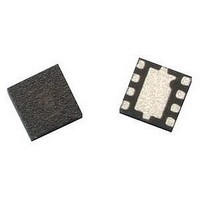
MGA-632P8-TR1G Avago Technologies US Inc., MGA-632P8-TR1G Datasheet

MGA-632P8-TR1G
Specifications of MGA-632P8-TR1G
Available stocks
Related parts for MGA-632P8-TR1G
MGA-632P8-TR1G Summary of contents
Page 1
... Small Leadless Package (TSLP) package. The compact footprint and low profile coupled with low noise, high gain, excellent input return loss and high linearity make the MGA-632P8 an ideal choice as an LNA for cellular in- frastructure for GSM, CDMA, W-CDMA and TD-SCDMA ap- plications. ...
Page 2
... MGA-632P8 Absolute Maximum Rating Symbol Parameter Vd Device Supply Voltage P (ON Input Power in,max (Vd = 4.0V, Vbias=4.0V) P (OFF Input Power in,max (Vd=4.0V, Vbias=0V) P Total Power Dissipation diss T Junction Temperature j T Storage Temperature STG [3] Thermal Resistance (Vd = 4.0V, Vbias=4.0V), θ Notes: 1. Operation of this device in excess of any of these limits may cause permanent damage. ...
Page 3
Electrical Specifications °C, Vd =4V @ 57mA, R1=300ohm unless otherwise specified. A Symbol Parameter and Test Condition Id Operational Current Gain Freq=1.75 GHz Freq=1.85 GHz Freq=1.95 GHz OIP3 Freq=1.75 GHz Freq=1.85 GHz Freq=1.95 GHz NF ...
Page 4
Typical Electrical Specifications at 3.5GHz °C, Vd =4V @ 57mA, R1=300ohm unless otherwise specified. A Symbol Parameter and Test Condition Gain Freq=3.5GHz OIP3 Freq=3.5GHz NF Freq=3.5GHz 50Ω OP1dB Freq=3.5GHz IRL Freq=3.5GHz ORL Freq=3.5GHz S12 Freq=3.5GHz Notes: 1. ...
Page 5
... MGA-632P8 Typical Performance T = +25 ° 4V 57mA, R1=300ohm unless stated otherwise 20mA 40mA 7 60mA 80mA 5 1.70 1.75 1.80 1.85 1.90 1.95 2.00 2.05 2.10 Frequency (GHz) Figure 5. Gain Vs Frequency and (mA) Figure 8. Gain Vs Id and -40°C 25°C 10 85°C 0 0.0 1.0 2.0 3.0 4 ...
Page 6
... MGA-632P8 Typical Performance T = +25 ° 4V 57mA, R1=300ohm unless stated otherwise -40°C -30°C 15 25°C 85°C 10 1.70 1.75 1.80 1.85 1.90 1.95 2.00 2.05 2.10 Frequency (GHz) Figure 14. OIP3 vs Frequency and Temperature -40°C -30°C 5 25°C 85° (mA) Figure 17. OIP3 vs Id and Temperature ...
Page 7
... MGA-632P8 Typical Performance for 1.5 GHz Matching T = +25 ° 4V 57mA A 20 Gain 1.2 1.3 1.4 1.5 1.6 1.7 1.8 Frequency (GHz) Figure 23. Gain and NF Vs Frequency MGA-632P8 Typical Performance for 2.6 GHz Matching T = +25 ° 4V 57mA Gain 2.3 2.4 2.5 2.6 2 ...
Page 8
Demo Board Layout Figure 32. Demo Board Layout Diagram - Recommended PCB material is 10 mils Rogers RO4350. - Suggested component values may vary according to layout and PCB material. Demo Board Schematic for Table 1 C7 Rbias RFin RFin ...
Page 9
Table 1 List 1 – Demo Board Component values for Demo board Schematic of Fig. 29. These component values are used when measuring electrical specifications and plots of Fig Fig. 21. List 2 – Demo Board Component values ...
Page 10
Load pull test set up Vbias C5 C6 Rbias C1 Input RFgnd C4 Vbias C7 Figure 34. Test setup for load pull data The input port is matched for good NF and IRL. Because of the high reverse isolation, any ...
Page 11
Measured results Test condition: 4V/57mA, 1.95GHz Refer to Table 1, List 1 for SMT component value and de- scription, unless otherwise stated. Γ Resistor, R1 160ohm 0.48 < 91.4° 56ohm 0.61 <134.2° 10kohm 0.40 < 150° Figure 35. Load pull ...
Page 12
Figure 36. Load pull contour plot for R1=56ohm Figure 37. Load pull contour plot for R1=10kohm 12 ...
Page 13
... MGA-632P8 Scattering Parameter and Noise Parameter Test Setup Figure 38. Test Setup for S & Noise Parameters data, C3=1.2pF (Rohm MCH155A1R2CK) Typical Noise Parameter, Vd=4V, Id=57mA, applicable to any R1 due to high reverse isolation Freq FMIN GAMMA (GHz) (dB) Mag 0.9 0.41 0.31 1.9 0.55 0.27 2 ...
Page 14
... MGA632P8 Typical Scattering Parameters, Vd=4V, Id=57mA, R1=91ohm Freq S11 (GHz) Mag Ang 0.1 0.97 -10.0 0.5 0.73 -39.0 0.9 0.53 -51.2 1.0 0.50 -52.8 1 ...
Page 15
... MGA632P8 Typical Scattering Parameters, Vd=4V, Id=57mA, R1=1.5kohm Freq S11 (GHz) Mag Ang 0.1 0.96 -10.0 0.5 0.75 -36.8 0.9 0.57 -50.3 1.0 0.54 -52.4 1 ...
Page 16
... MGA632P8 Typical Scattering Parameters, Vd=4V, Id=57mA, R1=10kohm Freq S11 (GHz) Mag Ang 0.1 0.96 -9.9 0.5 0.75 -36.8 0.9 0.57 -50.7 1.0 0.54 -52.8 1.5 0.43 -59.0 1.9 0.39 -61.6 2.0 0.38 -61.8 2.5 0.36 -63.7 3.0 0.34 -64.0 3.5 0.33 -65 ...
Page 17
... Ordering Information Part Number No. of Devices MGA-632P8-TR1G 3000 MGA-632P8-TR2G 10000 MGA-632P8-BLKG 100 TSLP2X2 Package Dimension PCB Land Pattern and Stencil Design 2.80 (110.24) 0.70 (27.56) 0.25 (9.84) PIN 1 ∅ 0.20 (7.87) Solder + mask 0.60 (23.62) RF transmission 0.80 (31.50) line 0.15 (5.91) ...
Page 18
Device Orientation REEL USER FEED DIRECTION COVER TAPE Tape Dimensions 10° Max A 0 DESCRIPTION CAVITY LENGTH WIDTH DEPTH PITCH BOTTOM HOLE DIAMETER PERFORATION DIAMETER PITCH POSITION CARRIER TAPE WIDTH THICKNESS COVER TAPE WIDTH TAPE ...


