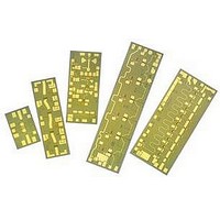
AMMC-5023-W50 Avago Technologies US Inc., AMMC-5023-W50 Datasheet - Page 2

AMMC-5023-W50
Manufacturer Part Number
AMMC-5023-W50
Description
IC MMIC AMP LO NOISE 23GHZ
Manufacturer
Avago Technologies US Inc.
Type
General Purposer
Datasheet
1.AMMC-5023-W50.pdf
(9 pages)
Specifications of AMMC-5023-W50
Function
Amplifier
Gain
23dB
Noise Figure Typ
2.3dB
Supply Current
28mA
Supply Voltage Range
3V To 7V
Frequency Max
26.5GHz
Frequency Min
21.2GHz
Supply Voltage Max
7V
Supply Voltage Min
3V
Number Of Channels
1
Frequency (max)
26.5GHz
Output Power
10@26500MHzdBm
Power Supply Requirement
Single
Single Supply Voltage (min)
3V
Single Supply Voltage (typ)
5V
Single Supply Voltage (max)
7V
Dual Supply Voltage (min)
Not RequiredV
Dual Supply Voltage (typ)
Not RequiredV
Dual Supply Voltage (max)
Not RequiredV
Operating Temperature Classification
Military
Operating Temp Range
-55C to 140C
Lead Free Status / RoHS Status
Lead free / RoHS Compliant
Lead Free Status / RoHS Status
Lead free / RoHS Compliant, Lead free / RoHS Compliant
AMMC-5023 DC Specifications/Physical Properties
Symbol
V
V
I
I
θ
Notes:
1. Backside ambient operating temperature T
2. Open circuit voltage at V
3. Channel-to-backside Thermal Resistance (θ
RF Specifications
(V
Symbol
|S
∆|S
RL
RL
|S
P
P
OIP3
NF
Note:
4. 100% on-wafer RF test is done at frequency = 21.2, 22.4, 23.6, 24.5, 25.5 and 26.5 GHz, except as noted.
2
D1
D1
ch-b
-1dB
sat
D1
G1
21
12
, I
+I
at backside temperature (T
G1
in
out
, V
, V
|
|
21
D2
2
2
D2
= V
|
G2
D2
2
G2
= Open, V
Parameters and Test Conditions
Recommended Drain Supply Voltage
Gate Supply Voltage
(V
Input and Output Stage Drain Supply Current
(V
Total Drain Supply Current
(V
Thermal Resistance
Parameters and Test Conditions
Small-signal Gain
Small-signal Gain Flatness
Input Return Loss
Output Return Loss
Isolation
Output Power @ 1 dB Gain Compression
f = 23 GHz
Saturated Output Power
(@ 3 dB Gain Compression)
Output 3
Rf
Noise Figure
D1
G1
G1
in1
= V
= V
≤ V
[4]
= Rf
G2
G2
D1(max)
D1
in2
= Open, V
= Open, V
rd
G1
= V
= -20 dBm, ∆f = 2 MHz 25.5 GHz
Order Intercept Point, 22.4 GHz
, V
and V
b
) = 25°C calculated from measured data.
D2
D2
= 5V, I
≤ V
G2
D1
when V
[3]
D1
[2]
D2(max)
= V
(Backside temperature, T
= V
D1
D2
D2
)
D1
+ I
= 5 V)
= 5 V)
A
ch-b
and V
= 25°C unless otherwise noted.
D2
) = 66°C/W at T
= 28 mA, Z
D2
are 5 Volts.
22 GHz
25 GHz
[1]
channel
in
= Z
b
= 25°C)
(T
0
c
= 50Ω)
) = 150°C as measured using the liquid crystal method. Thermal Resistance
Units
dB
dB
dB
dB
dB
dBm
dBm
dB
dB
21.2–23.6 GHz
Min.
21
10
9
40
Typ.
23.6
±1.5
12
12
50
9.5
10.5
18
2.3
Units
V
V
mA
mA
°C/W
Max.
28
2.8
Min.
3
13
24.5–26.5 GHz
Min.
17
10
10
40
Typ.
5
0.8
14
28
44
Typ.
19
±1.2
11.5
17
43
10
11.5
24
2.3
Max.
7
35
Max.
25
2.8


