AMMC-6430-W50 Avago Technologies US Inc., AMMC-6430-W50 Datasheet
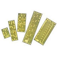
IC MMIC 1W POWER AMP 26-33GHZ

AMMC-6430-W50

Manufacturer Part Number
AMMC-6430-W50
Description
IC MMIC 1W POWER AMP 26-33GHZ
Manufacturer
Avago Technologies US Inc.
Type
Power Amplifierr
Datasheet

Specifications of AMMC-6430-W50

Function
Amplifier
Frequency Max
33GHz
Frequency Min
25GHz
Supply Voltage Max
7V
Number Of Channels
1
Frequency (max)
33GHz
Output Power
28.5@32000MHzdBm
Power Supply Requirement
Single
Single Supply Voltage (typ)
5.5V
Dual Supply Voltage (min)
Not RequiredV
Dual Supply Voltage (typ)
Not RequiredV
Dual Supply Voltage (max)
Not RequiredV
Supply Current
1000@5VmA
Lead Free Status / RoHS Status
Lead free / RoHS Compliant
Lead Free Status / RoHS Status
Lead free / RoHS Compliant, Lead free / RoHS Compliant

Available stocks

Company
Part Number
Manufacturer
Quantity
Price
Part Number:
AMMC-6430-W50
Manufacturer:
AVAGO/安华高
Quantity:
20 000
AMMC - 6430
25 - 33 GHz Power Amplifier
Data Sheet
Description
The AMMC-6430 MMIC is a broadband nearly 1W power
amplifier designed for use in transmitters that operate
in various frequency bands between 25GHz and 33GHz.
This MMIC optimized for linear operation with an output
third order intercept point (OIP3) of 37dBm. At 30GHz it
provides 29dBm of output power (P-1dB) and 17dB of
gain. The device has input and output matching circuitry
for use in 50 Ω environments. The AMMC-6430 also inte-
grates a temperature compensated RF power detection
circuit that enables power detection of 0.3V/W. DC bias is
simple and the device operates on widely available 5.5V
for current supply (negative voltage only needed for Vg).
It is fabricated in a PHEMT process for exceptional power
and gain performance. For improved reliability and
moisture protection, the die is passivated at the active
areas.
AMMC-6430 Absolute Maximum Ratings
Note:
1. Operation in excess of any one of these conditions may result in permanent damage to this device.
Symbol
V
V
I
P
T
T
T
dq
ch
stg
max
d
in
g
Note: These devices are ESD sensitive. The following precautions are strongly recommended. Ensure
that an ESD approved carrier is used when dice are transported from one destination to another.
Personal grounding is to be worn at all times when handling these devices
Parameters/Conditions
Positive Drain Voltage
Gate Supply Voltage
Drain Current
CW Input Power
Operating Channel Temp.
Storage Case Temp.
Maximum Assembly Temp (60 sec max)
[1]
Chip Size: 2500 x 1750 µm (100 x 69 mils)
Chip Size Tolerance: ± 10µm (±0.4 mils)
Chip Thickness: 100 ± 10µm (4 ± 0.4 mils)
Pad Dimensions: 100 x 100 µm (4 ± 0.4 mils)
Features
• Wide frequency range: 25 - 33 GHz
• High gain: 17 dB
• Power: @30 GHz, P-1dB=29 dBm
• Highly linear: OIP3=37dBm
• Integrated RF power detector
• 5.5 Volt, -0.7 Volt, 900mA operation
Applications
• Microwave Radio systems
• Satellite VSAT and DBS systems
• LMDS & Pt-Pt mmW Long Haul
• 802.16 & 802.20 WiMax BWA
• WLL and MMDS loops
• Can be driven by AMMC-6345, increasingluding overall
gain.
Units
V
V
mA
dBm
°C
°C
°C
Min.
-3
-65
Max.
7
0.5
1500
23
+150
+150
+300

Related parts for AMMC-6430-W50

AMMC-6430-W50 Summary of contents

Page 1

... It is fabricated in a PHEMT process for exceptional power and gain performance. For improved reliability and moisture protection, the die is passivated at the active areas. AMMC-6430 Absolute Maximum Ratings Symbol Parameters/Conditions V Positive Drain Voltage d V Gate Supply Voltage ...

Page 2

... AMMC-6430 DC Specifications/Physical Properties Symbol Parameters and Test Conditions I Drain Supply Current dq (under any RF power drive and temperature set for Gate Supply Operating Voltage 900 (mA)) d(Q) q [2] Thermal Resistance ch-b (Backside temperature, T Notes: 1. Ambient operational temperature T =25°C unless otherwise noted Channel-to-backside Thermal Resistance (θ at backside temperature ( 25°C calculated from measured data AMMC-6430 RF Specifications T = 25°C, V =5.5V, I 900 mA d(Q)= Symbol Parameters and Test Conditions [4] Gain ...

Page 3

... AMMC-6430 Typical Performances (T = 25° NOTE: These measurements are Ω test environment. Aspects of the amplifier performance may be improved over a more narrow bandwidth by application of additional conjugate, linearity, or power matching S21[dB] S12[dB Frequency [GHz] Figure 1. Typical Gain and Reverse Isolation Frequency [GHz] Figure 4. Typical Noise Figure 0 S11_20 S11_-40 S11_85 -5 -10 -15 -20 - Frequency[GHz] Figure 7. Typical S11 over temperature 3 =5 ...

Page 4

P-1_85deg P-1_20deg 22 P-1_-40deg Frequency [GHz] Figure 10. Typical One dB Compression over temperature [1] Typical Scattering Parameters , (T = 25° S11 Freq GHz ...

Page 5

Biasing and Operation The recommended quiescent DC bias condition for optimum efficiency, performance, and reliability is Vd=5 volts with Vg set for Id=950 mA. Minor improvements in performance are possible depending on the application. The drain bias voltage range 5.5V. A single DC gate supply connected to Vg will bias all gain stages. Muting can be accomplished by setting Vg and / the pinch-off voltage Vp. An optional output power detector network is also provided. The differential voltage between ...

Page 6

... DET_R Figure 11. AMMC-6430 Schematic Figure 12. AMMC-6430 Bonding pad locations Three stage 0.5W power amplifier DQ DET_O RF out ...

Page 7

... DET_O AMMC-6430 V d RFO DET_R 1µ Ordering information: 1 AMMC-6430-W10 = 10 devices per tray AMMC-6430-W50 = 50 devices per tray 0.1 0.01 0.001 30 35 www.avagotech.com RFOutput Notes: 1µ F capacitors on gate and 1. drain lines not shown required. Vg connection is recommended 2. on both sides for devices operating at or above P1dB. ...

Related keywords