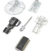
ADNK-3043-ND24 Avago Technologies US Inc., ADNK-3043-ND24 Datasheet - Page 4

ADNK-3043-ND24
Manufacturer Part Number
ADNK-3043-ND24
Description
WIRELESS MOUSE DESIGN KIT
Manufacturer
Avago Technologies US Inc.
Type
Wireless Mouse Development Kitr
Datasheet
1.ADNK-3043-ND24.pdf
(16 pages)
Specifications of ADNK-3043-ND24
Frequency
2.4GHz
Wireless Frequency
2.4 GHz
Interface Type
USB
For Use With/related Products
ADNS-3043
Lead Free Status / RoHS Status
Lead free / RoHS Compliant
Lead Free Status / RoHS Status
Lead free / RoHS Compliant, Lead free / RoHS Compliant
Serial Peripheral Interface (SPI)
The MSP430F1222 provides a dedicated hardware-based
Serial Peripheral Interface (SPI). The three-wire interface
supports byte serial communication in either Master or
Slave mode. In this reference design the MSP430F1222
always acts as the master and initiates all SPI communi-
cations with external SPI device(s), in this case the ADNS-
3040 and the nRF2401.
Z-Wheel Quadrature Encoder
A standard two-channel, incremental optical quadrature
encoder and an IR LED provide the scroll wheel function.
The MSP430F1222 manages the IR LED directly. Since
achieving low-power consumption is one of the main ob-
jectives, the optical LED is only enabled when the MSP430
needs to read the output states of the optical quadrature
encoder to the MSP430 port pins while in ACTIVE mode.
The optical LED is pulsed on for approximately 40 µsec
every 2 msec while in ACTIVE mode to read the current
position of the scroll wheel, thus saving power since the
optical LED is only on for a duty cycle of 2%. The outputs
of the two-channel quadrature encoder are squarewaves
that are 90° out of phase. The phase relationship of these
signals encodes the directions of scroll wheel rotations.
Within the MSP430, an internal Quadrature Encoder Pulse
(QEP) state machine interprets these signals and incre-
ments or decrements a counter based on the direction
and movement of the scroll wheel.
Wireless RF Technology
In order to provide the maximum flexibility the reference
design mouse utilizes two circuit boards. The main board
consists of the ADNS-3040 navigation sensor/LED, the
MSP430F1222 microcontroller, the scroll wheel and
button switches. A 10-pin header connects the main
board to the RF daughter card. The Nordic nRF2401 2.4
GHz transmitter and its associated circuit including the
antenna resides on the daughter card. The 10-pin header
provides the SPI, regulated Vdd and unregulated battery
voltage (for possible future applications). The nRF2402 is
a single-chip transmitter for the world wide 2.4-2.5 GHz
ISM band. The transmitter consists of a fully integrated
4
frequency synthesizer, a power amplifier, a crystal oscilla-
tor and a modulator. The output power and channel are
programmed through the SPI. Chip Select (CS) is used to
enable the nRF2402 when the microcontroller is ready
to pass it the motion or button switch data. Once the
data has been loaded into its input buffer the nRF2402
manages the transmission and returns to power down
mode to conserve battery power. Typical power consump-
tion is 10 mA at -5 dBm of output power.
The nRF2402 has two transmit modes:
• ShockBurst
• Direct Mode
In this reference design ShockBurstTM is used to capital-
ize on its benefit. It utilizes the on-chip FIFO to accept SPI
data at the microcontroller operating rate but transmit at
very high rate (up to 1 Mbps). The short transmission time
enables extreme power saving. For detailed description
of the ShockBurstTM technology please refer to: www.
nordicsemi.no/
High-frequency PCB layout:
A well-designed PCB is necessary to achieve good RF
performance. A fully qualified RF layout for the nRF2402
and it’s surrounding components, including matching
networks for the antenna can be downloaded from:
www.nordicsemi.no
A PCB with a minimum of two layers including a ground
plane is recommended for optimum performance.
The nRF2402 dc supply should be well filtered and
decoupled as close as possible to the Vdd pins with high
performance RF capacitors. Specifically a high-grade
SMD tantalum capacitor (e.g. 4.7 µF) should be used in
parallel with the smaller-value high-frequency bypassing
capacitors. The nRF2402 should have its own branch of
well-filtered supply voltage, routed separately from the
supply voltage for the digital circuitry.
Full swing digital signals should not be routed close to the
crystal or the power supply lines.
TM


