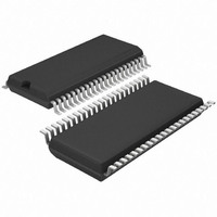
T4260-ILSH Atmel, T4260-ILSH Datasheet - Page 24

T4260-ILSH
Manufacturer Part Number
T4260-ILSH
Description
IC AM/FM FRONT END W/PLL 44SSOP
Manufacturer
Atmel
Datasheet
1.T4260-ILQH.pdf
(34 pages)
Specifications of T4260-ILSH
Frequency
AM, FM
Modulation Or Protocol
AM, FM
Applications
AM/FM Radio Receiver
Current - Receiving
85mA
Data Interface
PCB, Surface Mount
Antenna Connector
PCB, Surface Mount
Voltage - Supply
8 V ~ 10 V
Operating Temperature
-40°C ~ 85°C
Package / Case
44-SSOP
Lead Free Status / RoHS Status
Lead free / RoHS Compliant
Features
-
Sensitivity
-
Memory Size
-
Data Rate - Maximum
-
10.22 Permitted DAC Conditions
24
T4260
The offset of DAC1 and DAC2 has a range of approximately +0.98V to -0.99V. This range is
divided into 127 steps. One step is approximately 1.97 /127 = 15.52 mV. The offset of DAC1 can
be controlled by the bits 24 to bit 30 (2
the bits 52 to bit 58 (2
Table 10-26. Offset of DAC1, 2
Note:
The internal operation amplifier of the DACs should not operate with a too high internal differ-
ence voltage at their inputs. This means that a voltage difference higher than 0.5V at the internal
OP input should be avoided in operation mode. The respective output OP in the DAC is neces-
sary for the addition and amplification of the tuning voltage (at pin 18) with the desired voltage
gain and offset value.
If the tuning voltage reaches a high value e.g. 9V, with a gain setting of 2 times VTUNE and an
offset of +1V, then the output OP of the DAC should reach the (calculated) voltage of 19V. The
supply voltage of e.g. 10V, however, limits the output voltage (of the DAC) to 10V maximum.
Due to the (limiting) supply voltage and the internal gain resistance ratio of 6, the missing 9V
(calculated voltage - V
for a longer period of time.
As long as the calculated DAC output voltage value does not exceed the supply voltage value by
more than 3V, no damages should occur during the product’s lifetime as the input voltage of the
internal OP input voltage does not exceed 0.5V.
VTUNE
(9V
This means when having a gain factor of 2 and an offset value of 1V, the tuning voltage should
not exceed 6V.
Approximately
Approximately
Offset DAC1
Offset DAC2
2 + 1V) < 10V + 3V (condition not allowed)
–0.0120V
–0.9576V
–0.9733V
–0.9890V
Gain = 58 (intermediate position)
0.9815V
0.9659V
0.9512V
0.9353V
DAC gain factor + DAC offset < V
...
...
0
s
) cause a voltage of 1.5V at the OP input. This condition may not remain
to 2
B30
B58
6
0
0
0
0
1
1
1
1
) as given in
B29
B57
...
...
0
0
0
0
0
1
1
1
0
to 2
Table
B28
B56
...
...
0
0
0
0
0
1
1
1
S
6
) and the offset gain of DAC2 can be controlled by
+ 3V
10-26.
B26
B55
...
...
0
0
0
0
0
1
1
1
B26
B54
...
...
0
0
0
0
0
1
1
1
B25
B53
...
...
0
0
1
1
0
0
1
1
B24
B52
...
...
0
1
0
1
0
1
0
1
Decimal Offset
Decimal Offset
4528N–AUDR–11/09
125
126
127
64
...
...
0
1
2
3


