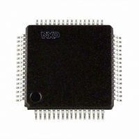
TEF6721HL/V1S,518 NXP Semiconductors, TEF6721HL/V1S,518 Datasheet - Page 10

TEF6721HL/V1S,518
Manufacturer Part Number
TEF6721HL/V1S,518
Description
IC FRONT END DGTL CAR RAD 64LQFP
Manufacturer
NXP Semiconductors
Datasheet
1.TEF6721HLV1S518.pdf
(48 pages)
Specifications of TEF6721HL/V1S,518
Modulation Or Protocol
AM, FM, WB
Applications
AM/FM Radio Receiver
Data Interface
PCB, Surface Mount
Antenna Connector
PCB, Surface Mount
Voltage - Supply
5V, 8.5V
Operating Temperature
-40°C ~ 85°C
Package / Case
64-LQFP
Lead Free Status / RoHS Status
Lead free / RoHS Compliant
Features
-
Frequency
-
Sensitivity
-
Memory Size
-
Data Rate - Maximum
-
Current - Receiving
-
Lead Free Status / RoHS Status
Lead free / RoHS Compliant, Lead free / RoHS Compliant
Other names
935288831518
Philips Semiconductors
8. I
TEF6721HL_4
Product data sheet
2
C-bus protocol
7.10 FM/AM RF AGC buffer
8.1 I
minimum JFET drain source voltage is controlled by a Direct Current (DC) feedback loop
(pin VAMCASFB) in order to limit the cascode AGC range to 10 dB. If the cascode AGC is
not required, a simple RF AGC loop is possible by using only a PIN diode. In some
conditions, noise behavior will increase. In this case pins VAMCAS and VAMCASFB have
to be left open-circuit. In FM mode, the cascode switches off the JFET bias current to
reduce the total power consumption.
The AGC detection points for AM RF AGC are at the AM mixer input (threshold
programmable via the I
threshold).
In FM mode the AM AGC can be activated via the I
1 mA from the PIN diode.
This output current can be used to reduce the gain of active antennas before start of
RF AGC.
The output (open-collector) sinks a current which in AM mode is proportional to the
voltage at pin TRFAMAGC and in FM mode proportional to the RF level detector voltage
(pin TFMAGC) inside the FM AGC.
SDA and SCL HIGH and LOW levels are specified according to a 3.3 V I
pins tolerate also thresholds of a 5 V bus.
The standard I
IC addresses:
Structure of the I
Subaddresses are not used.
The second I
resistor to ground. The third I
pin ADDRSEL via a 33 k resistor to ground.
The maximum bit rate for this device is 100 kbit/s.
The I
BUSENABLE is HIGH the communication with the device is active; if pin BUSENABLE is
LOW the signals on the I
used to communicate with other devices on the same I
change while bus communication takes place.
2
•
•
•
C-bus specification
1st IC address C2h: 1100001 R/W
2nd IC address C0h: 1100000 R/W
3rd IC address C4h: 1100010 R/W.
2
C-bus interface is extended with an enable input (pin BUSENABLE). If pin
2
C-bus address can be selected by connecting pin ADDRSEL via a 120 k
2
C-bus specification is expanded by the following definitions.
2
C-bus logic: slave transceiver with auto increment.
Rev. 04 — 20 December 2005
2
C-bus) and the AM and FM IF AGC amplifier input (fixed
2
C-bus are ignored so that higher bit rates (> 100 kbit/s) can be
2
C-bus address can be selected by connecting
Car radio tuner front-end for digital IF
2
C-bus to sink a constant current of
2
C-bus. The enable signal must not
© Koninklijke Philips Electronics N.V. 2005. All rights reserved.
TEF6721HL
2
C-bus. The bus
10 of 48


