MRF24WB0MA/RM Microchip Technology, MRF24WB0MA/RM Datasheet - Page 14
MRF24WB0MA/RM
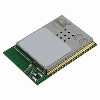
Manufacturer Part Number
MRF24WB0MA/RM
Description
TXRX RF 2.4GHZ PCB ANT 802.11B
Manufacturer
Microchip Technology
Specifications of MRF24WB0MA/RM
Frequency
2.4GHz
Data Rate - Maximum
1Mbps
Modulation Or Protocol
802.11 b
Applications
ISM
Power - Output
10dBm
Sensitivity
-91dBm
Voltage - Supply
2.7 V ~ 3.6 V
Current - Receiving
85mA
Current - Transmitting
154mA
Data Interface
PCB, Surface Mount
Antenna Connector
On-Board, Trace
Operating Temperature
0°C ~ 70°C
Package / Case
Module
Wireless Frequency
2.4 GHz
Interface Type
SPI, JTAG
Board Size
21 mm x 31 mm
Modulation
DSSS
Security
WEP, WPA-PSK, WPA-2-PSK
Operating Voltage
2.7 V to 3.6 V
Antenna
PCB Meander
Operating Temperature Range
0 C to + 70 C
Frequency Rf
2.4GHz
Transmit Power
9mW
Module Interface
SPI, 4-Wire
Modulation Type
DSSS
Data Rate Max
2Mbps
Supply Current
154mA
Supply Voltage Range
2.7V To 3.6V
Frequency Range
2.4GHz
Leaded Process Compatible
Yes
Rohs Compliant
Yes
For Use With/related Products
PIC18, PIC24, dsPIC33, PIC32
Lead Free Status / RoHS Status
Lead free / RoHS Compliant
Memory Size
-
Lead Free Status / Rohs Status
Lead free / RoHS Compliant
Available stocks
Company
Part Number
Manufacturer
Quantity
Price
Company:

Part Number:
MRF24WB0MA/RM
Manufacturer:
MICROCHIP
Quantity:
2 000


MRF24WB0MA/MRF24WB0MB
2.2
The internal regulators for the digital and analog core
power supplies are enabled by driving the HIBERNATE
pin high. Figure 2-2 shows the waveforms for the core
supplies when powering up the MRF24WB0MA/
MRF24WB0MB with a nominal 3.3V applied to VDD.
FIGURE 2-2:
2.3
The
power states. These are Hibernate, Sleep and Active
(two sub-states), as shown in Figure 2-3. The selection
of power state directly affects system behavior, as well
as overall power consumption or battery life. There is
also a “Standby” state that is not user-controlled.
2.3.1
An “Off” state is defined as no power applied to the
device. The Hibernate mode is the closest to controlled
off that the module can approach. It is controlled via the
HIBERNATE pin (high input puts the module into Hiber-
nate). When in Hibernate, the module only consumes
leakage current, but does not maintain state. Hibernate
has to be fully controlled by the PIC MCU and requires
the TCP/IP stack to restart on an awake. This state pro-
vides the best battery life for embedded products. Note
that entering Hibernate for intervals of less than 30 sec-
onds is not likely to save power. Battery life expectation
can be more than a year for devices operating on AA
cells that would be in Hibernate except to wake up
every hour for a small data transfer (<500 Bytes).
DS70632A-page 14
MRF24WB0MA/MRF24WB0MB
Power-On Sequence
Power States
HIBERNATE STATE
2.7 V
(System Dependent)
MRF24WB0MA/MRF24WB0MB POWER-ON SEQUENCE TIMING
Power On Ramp
V
DD
<5 ms
has
several
300 ms minimum
MRF24WB0MA
Preliminary
Internal Boot
There is an internal Power-on-Reset (POR) detect
which starts the boot sequence from the internal ROM
when the core is powered. After approximately 300 ms
from when the VDD supply is within specification, the
MRF24WB0MA/MRF24WB0MB is ready for operation.
2.3.2
The Sleep state is a low power dynamic state that auto-
matically implements the 802.11 Power Save feature.
In this mode, if enabled, the module will enter power
save mode when all activity is complete.
The module will wake autonomously to any PIC inter-
vention so it can check DTIM beacons from the Access
Point. If any traffic is listed as queued for the module,
then it will awaken and get the data from the Access
Point on the next possible opportunity. When data is
acquired, the module will interrupt the PIC microcon-
troller on a normal “data available” indication. If no data
is available on a DTIM check, the module reenters the
Power Save state until the next DTIM. The DTIM inter-
val is programmed at the Access Point. This state can
provide “as if on” behavior of the radio with a significant
power savings versus “always on”. The battery life
expectation of this mode is several days to several
weeks. This mode is characterized by a very low
latency (as low as 200 mS) to transfer data from the low
power state.
2.3.3
The Active state is identified as one of two states where
the radio circuitry is fully on. There is the Receive state
(RX ON) and the Transmit state (TX ON).
SLEEP STATE
ACTIVE STATE
Ready for
Operation
2010 Microchip Technology Inc.
Time
Related parts for MRF24WB0MA/RM
Image
Part Number
Description
Manufacturer
Datasheet
Request
R

Part Number:
Description:
Manufacturer:
Microchip Technology Inc.
Datasheet:
Part Number:
Description:
Manufacturer:
Microchip Technology Inc.
Datasheet:
Part Number:
Description:
Manufacturer:
Microchip Technology Inc.
Datasheet:
Part Number:
Description:
Manufacturer:
Microchip Technology Inc.
Datasheet:
Part Number:
Description:
Manufacturer:
Microchip Technology Inc.
Datasheet:
Part Number:
Description:
Manufacturer:
Microchip Technology Inc.
Datasheet:
Part Number:
Description:
Manufacturer:
Microchip Technology Inc.
Datasheet:
Part Number:
Description:
Manufacturer:
Microchip Technology Inc.
Datasheet: