SX1231IMLTRT Semtech, SX1231IMLTRT Datasheet
SX1231IMLTRT
Specifications of SX1231IMLTRT
Available stocks


Related parts for SX1231IMLTRT


SX1231IMLTRT Summary of contents
Page 1
... Automatic RF Sense with ultra-fast AFC Packet engine with CRC, AES-128 encryption and 66- byte FIFO Built-in temperature sensor and Low Battery indicator ORDERING INFORMATION Part Number SX1231IMLTRT QFN 24 Package - Operating Range [-40;+85°C] Pb-free, Halogen free, RoHS/WEEE compliant product Page 1 SX1231 DATASHEET ...
Page 2
... Over Current Protection ........................................................................................................................... 21 3.5. Receiver Description ..................................................................................................................................... 22 3.5.1. Block Diagram .......................................................................................................................................... 22 3.5.2. LNA - Single to Differential Buffer ............................................................................................................ 22 3.5.3. Automatic Gain Control ............................................................................................................................ 23 3.5.4. Quadrature Mixer - ADCs - Decimators.................................................................................................... 24 3.5.5. Channel Filter ........................................................................................................................................... 25 3.5.6. DC Cancellation ....................................................................................................................................... 26 3.5.7. Complex Filter - OOK ............................................................................................................................... 26 3.5.8. RSSI ......................................................................................................................................................... 26 Rev 3 - April 2010 Page 2 SX1231 DATASHEET Page www.semtech.com ...
Page 3
... Control ...................................................................................................................................................... 45 5.3. Digital IO Pins Mapping................................................................................................................................. 45 5.3.1. DIO Pins Mapping in Continuous Mode ................................................................................................... 46 5.3.2. DIO Pins Mapping in Packet Mode .......................................................................................................... 46 5.4. Continuous Mode .......................................................................................................................................... 47 5.4.1. General Description.................................................................................................................................. 47 5.4.2. Tx Processing........................................................................................................................................... 47 5.4.3. Rx Processing .......................................................................................................................................... 48 5.5. Packet Mode ................................................................................................................................................. 48 5.5.1. General Description.................................................................................................................................. 48 Rev 3 - April 2010 Page 3 SX1231 DATASHEET www.semtech.com ...
Page 4
... Chip Revisions ...................................................................................................................................................... 78 9.1. RC Oscillator Calibration............................................................................................................................... 78 9.2. Listen Mode................................................................................................................................................... 78 9.2.1. Resolutions............................................................................................................................................... 78 9.2.2. Exiting Listen Mode .................................................................................................................................. 79 9.3. OOK Floor Threshold Default Setting ........................................................................................................... 79 9.4. OCP Block..................................................................................................................................................... 79 9.5. AFC Control .................................................................................................................................................. 79 9.5.1. AfcAutoClearOn ....................................................................................................................................... 79 9.5.2. LowBetaAfcOn and LowBetaAfcOffset..................................................................................................... 79 10. Revision History .................................................................................................................................................... 80 Rev 3 - April 2010 Page 4 SX1231 DATASHEET www.semtech.com ...
Page 5
... Figure 33. Unlimited Length Packet Format ................................................................................................................ 51 Figure 34. CRC Implementation .................................................................................................................................. 56 Figure 35. Manchester Encoding/Decoding ................................................................................................................. 56 Figure 36. Data Whitening ........................................................................................................................................... 57 Figure 37. POR Timing Diagram ................................................................................................................................. 73 Figure 38. Manual Reset Timing Diagram ................................................................................................................... 74 Figure 39. +13dBm Schematic .................................................................................................................................... 74 Figure 40. +17dBm Schematic .................................................................................................................................... 75 Figure 41. Package Outline Drawing ........................................................................................................................... 76 Rev 3 - April 2010 Page 5 SX1231 DATASHEET Page www.semtech.com ...
Page 6
... Table 22. Common Configuration Registers ................................................................................................................. 61 Table 23. Transmitter Registers ................................................................................................................................... 64 Table 24. Receiver Registers ....................................................................................................................................... 65 Table 25. IRQ and Pin Mapping Registers ................................................................................................................... 67 Table 26. Packet Engine Registers .............................................................................................................................. 69 Table 27. Temperature Sensor Registers ..................................................................................................................... 72 Table 28. Test Registers .............................................................................................................................................. 72 Table 29. Crystal Specification ..................................................................................................................................... 73 Table 30. Chip Identification ......................................................................................................................................... 78 Table 31. Revision History ............................................................................................................................................ 80 Rev 3 - April 2010 Page 6 SX1231 DATASHEET Page www.semtech.com ...
Page 7
... Phase-Locked Loop POR Power On Reset RBW Resolution BandWidth RF Radio Frequency RSSI Received Signal Strength Indicator Rx Receiver SAW Surface Acoustic Wave SPI Serial Peripheral Interface SR Shift Register Stby Standby Tx Transmitter uC Microcontroller VCO Voltage Controlled Oscillator XO Crystal Oscillator XOR eXclusive OR Page 7 SX1231 DATASHEET www.semtech.com ...
Page 8
... ADVANCED COMMUNICATIONS & SENSING This product datasheet contains a detailed description of the SX1231 performance and functionality. Please consult the Semtech website for the latest updates or errata. Refer to section 9 of this document to identify chip revisions. 1. General Description The SX1231 is a single-chip integrated circuit ideally suited for today's high performance ISM band RF applications. The SX1231's advanced features set, including state of the art packet engine greatly simplifies system design whilst the high level of integration reduces the external BOM to a handful of passive decoupling and matching components ...
Page 9
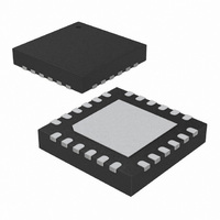
... Pin and Marking Diagram The following diagram shows the pin arrangement of the QFN package, top view. Notes yyww refers to the date code xxxxxx refers to the lot number Rev 3 - April 2010 Figure 2. Pin Diagram Figure 3. Marking Diagram Page 9 SX1231 DATASHEET www.semtech.com ...
Page 10
... SPI Clock input O MISO SPI Data output I MOSI SPI Data input I NSS SPI Chip select input O RXTX Rx/Tx switch control: high GND Ground I/O RFIO RF input / output - GND Ground O Optional high-power PA output - VR_PA Regulated supply for the PA Page 10 SX1231 DATASHEET Description www.semtech.com ...
Page 11
... Supply voltage Top Operational temperature range Clop Load capacitance on digital ports ML RF Input Level Rev 3 - April 2010 Description Description Page 11 SX1231 DATASHEET Min Max Unit -0.5 3.9 V -55 +115 ° +125 ° dBm Min Max Unit 1.8 3.6 V -40 +85 ° dBm www.semtech.com ...
Page 12
... MHz step 5 MHz step 7 MHz step 12 MHz step 20 MHz step 25 MHz step 19 FSTEP = FXOSC/2 Page 12 SX1231 DATASHEET Min Typ Max Unit - 0 1 1.25 1 Min Typ Max Unit 290 - 340 MHz 424 - 510 MHz 862 - 1020 MHz - 32 - MHz - 250 500 150 61 www.semtech.com ...
Page 13
... Min Typ Max Unit - -118 - dBm - -114 - dBm - -105 - dBm - -120 - dBm - -112 -109 dBm -13 - -45 - dBm - -40 - dBm - -32 - dBm - -36 - dBm - -33 - dBm - -25 - dBm - -45 - dBm - -40 - dBm - -32 - dBm - +75 - dBm - +35 - dBm - +20 - dBm -23 -18 - dBm 2.6 - 500 kHz www.semtech.com ...
Page 14
... BT=0.5 . Measurement conditions as defined by EN 300 220-1 V2.1.1 Frequency Synthesizer enabled, PaRamp = 10 us 4.8 kb/s. Page 14 SX1231 DATASHEET 1 3.0 ms 163 us 4.8 ms 265 bit - 4 bit - 2 bit - -115 - dBm - 0 - dBm Min Typ Max Unit - +13 - dBm - -18 - dBm - +17 - dBm - +/-0 -95 - dBc -37 dBm - 120 - us www.semtech.com ...
Page 15
... MOSI change to SCK rising edge from SCK rising edge to MOSI change from NSS falling edge to SCK rising edge from SCK falling edge to NSS rising edge, normal mode Page 15 SX1231 DATASHEET Min Typ Max Unit 0 VDD - - 0.2 VDD 0 VDD - - 0.1 VDD - - 10 MHz 250 - - ns www.semtech.com ...
Page 16
... XTA (pin 4). XTB (pin 5) should be left open. The peak-peak amplitude of the input signal must never exceed 1.8 V. Please consult your TCXO supplier for an appropriate value of decoupling capacitor, C Rev 3 - April 2010 . D XTA XTB NC TCXO OP 32 MHz Vcc Vcc GND C D Figure 4. TCXO Connection Page 16 SX1231 DATASHEET www.semtech.com ...
Page 17
... The Frf setting is split across 3 bytes. A change in the center frequency will only be taken into account when the least significant byte FrfLsb in RegFrfLsb is written. This allows for more complex modulation schemes such as m- ary FSK, where frequency modulation is achieved by changing the programmed RF frequency. Rev 3 - April 2010 F XOSC --------------- - = F STEP 19 2 × = Frf STEP Page 17 SX1231 DATASHEET www.semtech.com ...
Page 18
... A lock indication signal can be made available on some of the DIO pins, and is toggled high when the PLL reaches its locking range. Please refer to Table 19 and Table 20 to map this interrupt to the desired pins. Rev 3 - April 2010 5 ------------------- - = T PLLAFC PLLBW Page 18 SX1231 DATASHEET www.semtech.com ...
Page 19
... In Packet mode or in Continuous mode with Gaussian filtering enabled (refer to section 5.5 for details), the Bit Rate (BR) is controlled by bits BitRate in RegBitrate: Amongst others, the following Bit Rates are accessible: Rev 3 - April 2010 LNA RFIO Receiver Chain PA0 PA1 PA_BOOST PA2 Figure 5. Transmitter Block Diagram F XOSC ------------------- - = BR BitRate Page 19 SX1231 DATASHEET Local Oscillator www.semtech.com ...
Page 20
... Page 20 SX1231 DATASHEET Actual BR OOK (b/s) 1.2 kbps 1200.015 2.4 kbps 2400.060 4.8 kbps 4799.760 9.6 kbps 9600.960 19.2 kbps 19196.16 38415.36 76738.60 153846.1 57553.95 115107.9 12.5 kbps 12500.00 25 kbps 25000.00 50000.00 100000.0 150234.7 200000.0 250000.0 299065.4 32.768 kbps 32753.32 www.semtech.com ...
Page 21
... The current clamping value is controlled by OcpTrim bits in RegOcp, and is calculated with the following formula: Rev 3 - April 2010 Mode -18 to +13 dBm -18 to +13 dBm -14 to +17 dBm Reserved × OcpTrim Imax mA Page 21 SX1231 DATASHEET Power Range Pout Formula -18 dBm + OutputPower -18 dBm + OutputPower -14 dBm + OutputPower www.semtech.com ...
Page 22
... Any of the below, set by the AGC loop Max gain Max gain - 6 dB Max gain - 12 dB Max gain - 24 dB Max gain - 36 dB Max gain - 48 dB Reserved Page 22 SX1231 DATASHEET CORDIC Complex Filter Phase FSK Output Demodulator Module RSSI Output Demodulator Bypassed in FSK Gain Setting - www.semtech.com OOK ...
Page 23
... Lower Linearity Lower Noise Figure The following table summarizes the performance (typical figures) of the complete receiver: Rev 3 - April 2010 7dB 11dB Figure 7. AGC Thresholds Settings Page 23 SX1231 DATASHEET Pin [dBm] 9dB 11dB G5 G6 Lower Sensitivity Higher Linearity Higher Noise Figure www.semtech.com ...
Page 24
... Rev 3 - April 2010 Gain Receiver Performance (typ) Setting P NF -1dB [dB] [dBm] G1 -37 G2 -31 G3 -26 G4 -14 G5 >-6 G6 >0 th order continuous-time Sigma-Delta Analog to Digital Converters (ADC). Their Page 24 SX1231 DATASHEET IIP3 IIP2 [dBm] [dBm] 7 -18 +35 13 - +62 36 +13 +68 44 +20 +75 www.semtech.com ...
Page 25
... Page 25 SX1231 DATASHEET OOK 1.3 1.6 2.0 2.6 3.1 3.9 5.2 6.3 7.8 10.4 12.5 15.6 20.8 25.0 31.3 41.7 50.0 62.5 83.3 100.0 125.0 166.7 200.0 250.0 www.semtech.com ...
Page 26
... Phase output: used by the FSK demodulator and the AFC blocks. Amplitude output: used by the RSSI block, for FSK demodulation, AGC and automatic gain calibration purposes. Rev 3 - April 2010 × 4 RxBw ----------------------------------------- - = DccFreq × 2π 2 Q(t) Real-time Magnitude Real-time Phase I(t) Figure 8. Cordic Extraction Page 26 SX1231 DATASHEET www.semtech.com ...
Page 27
... BR Zoom Zoom Decay defined in OokPeakThreshStep Period as defined in OokPeakThreshDec Figure 9. OOK Peak Demodulator Description Page 27 SX1231 DATASHEET ‘’Peak -6dB’’ Threshold ‘’Floor’’ threshold defined by OokFixedThresh Noise floor of receiver Time Fixed 6dB difference www.semtech.com ...
Page 28
... Average Threshold: Data supplied by the RSSI block is averaged, and this operation mode should only be used with DC-free encoded data. Rev 3 - April 2010 Set SX1231 in OOK Rx mode Adjust Bit Rate, Channel filter BW Default OokFixedThresh setting No input signal Continuous Mode Monitor DIO2/DATA pin Increment OokFixedThresh Glitch activity on DATA ? Optimization complete Figure 10. Floor Threshold Optimization Page 28 SX1231 DATASHEET www.semtech.com ...
Page 29
... This function provides information about the frequency error of the local oscillator (LO) compared with the carrier frequency of a modulated signal at the input of the receiver. When the FEI block is launched, the frequency error is measured and the Rev 3 - April 2010 DATA DCLK Figure 11. Bit Synchronizer Description Page 29 SX1231 DATASHEET www.semtech.com ...
Page 30
... Upon user request, by setting bit AfcStart in RegAfcFei, if AfcAutoOn = 0 Rev 3 - April 2010 ⎛ ⎞ BR × ------ - = ⎝ ⎠ DEV 2 × = FEI F FeiValue STEP SX1231 in Rx mode Preamble-modulated input signal Signal level > Sensitivity Set FeiStart = 1 No FeiDone = 1 Yes Read FeiValue Figure 12. FEI Process Page 30 SX1231 DATASHEET www.semtech.com ...
Page 31
... When the optimized AFC routine is enabled, the receiver startup time can be computed as follows (refer to section 4.2.3): TS_RE_AGC&AFC (optimized AFC) = Tana + 4.Tcf + 4.Tdcc + 3.Trssi + 2.Tafc + 2.Tpllafc Rev 3 - April 2010 Offset = LowBetaAfcOffset x 488 Hz TX AfcValue Standard AFC AfcLowBetaOn = AfcValue Optimized AFC AfcLowBetaOn = 1 f After AFC Figure 13. Optimized AFC (AfcLowBetaOn=1) Page 31 SX1231 DATASHEET RX & LowBetaAfcOffset f www.semtech.com ...
Page 32
... Timeout interrupt is generated TimeoutRssiThresh Tbit after RssiThreshold flag has been raised. This timeout interrupt can be used to warn the companion processor to shut down the receiver and return to a lower power mode. Rev 3 - April 2010 ° -1 C/Lsb ° - t+1 Ambient Figure 14. Temperature Sensor Response Page 32 SX1231 DATASHEET ° +85 C www.semtech.com ...
Page 33
... FS Mode Transmit Mode Frequency synthesizer and transmitter Receive Mode Frequency synthesizer and receiver x Listen Mode = TS_OSC + TS_FS + TS_TR = TS_OSC + TS_FS + TS_RE = TS_OSC + TS_FS + TS_RE_AGC = TS_OSC + TS_FS + TS_RE_AGC&AFC Page 33 SX1231 DATASHEET Enabled blocks None Frequency synthesizer See Listen Mode, section 4.3 www.semtech.com ...
Page 34
... The startup times of the receiver can be calculated from the following: Rev 3 - April 2010 μ × PaRamp 1 μ × Tbit 2 TS_TR 1.25 x PaRamp Analog 0.5 x Tbit (only in FSK group delay mode Figure 15. Tx Startup, FSK and OOK Page 34 SX1231 DATASHEET 1 × Tbit 2 , Transmission of Packet www.semtech.com ...
Page 35
... Tcf Tdcc Trssi The LNA gain is adjusted by Carrier Frequency is adjusted the AGC, according to the RSSI result PLL Channel Filter’s DC Cutoff’s AFC Reception of Packet lock group delay group delay Tafc Tpllafc Tcf Tdcc (aka TS_RSSI) www.semtech.com by the AFC ...
Page 36
... Change the carrier frequency in the RegFrf registers Program the SX1231 in FS mode (2) Program the SX1231 in FS mode (3) Turn the transceiver back to Rx mode (4) Respect the Rx start procedure, described in section 4.2.4 Note all sequences described above are assuming that the sequencer is turned on (SequencerOff=0 in RegOpMode). Rev 3 - April 2010 Page 36 SX1231 DATASHEET www.semtech.com ...
Page 37
... The time during which the receiver is on and waits for a signal is given ListenIdle (denoted t in the following text) are fixed by two parameters from the ListenX = ⋅ ListenCoef X Listen ListenX Min duration Max duration ( ListenCoef = ListenCoef = 255 ) 64 us 4.1 ms 0.26 s Page 37 SX1231 DATASHEET Rx time t ListenRx solX www.semtech.com ...
Page 38
... Mode. Listen mode stops and must be disabled. Chip stays in Rx mode until PayloadReady or Timeout interrupt occurs. Listen mode then 10 resumes in Idle state. FIFO content is lost at next Rx wakeup. Rev 3 - April 2010 Input Signal Power SyncAddressMatch >= RssiThreshold Required Not Required Required Required Description Page 38 SX1231 DATASHEET www.semtech.com ...
Page 39
... For applications enduring large temperature variations, and for which the power supply is never removed, RC calibration can be performed upon user request. RcCalStart in RegOsc1 can be used to trigger this calibration, and the flag RcCalDone will be set automatically when the calibration is over. Rev 3 - April 2010 Idle Rx Idle Rx Idle Rx Page 39 SX1231 DATASHEET Mode Idle Rx www.semtech.com ...
Page 40
... Automatic reception (AutoRx) : Mode = Rx, IntermediateMode = Sleep, EnterCondition = CrcOk, ExitCondition = falling edge of FifoNotEmpty Automatic reception of acknowledge (AutoRxAck): Mode = Tx, IntermediateMode = Rx, EnterCondition = PacketSent, ExitCondition = CrcOk ... Rev 3 - April 2010 Intermediate State defined by IntermediateMode EnterCondition Final state defined By Mode in RegOpMode Figure 21. Auto Modes of Packet Handler Page 40 SX1231 DATASHEET ExitCondition www.semtech.com ...
Page 41
... Depending on the optional features activated (CRC, AES, etc) the maximum payload length is limited to FIFO size, 255 bytes or unlimited. Each of these data operation modes is described fully in the following sections. Rev 3 - April 2010 CONTROL PACKET FIFO HANDLER (+SR) Page 41 SX1231 DATASHEET DIO0 DIO1 DIO2 DIO3 DIO4 DIO5 SPI NSS SCK MOSI MISO www.semtech.com ...
Page 42
... In FIFO mode, if the address was the FIFO address then the bytes will be written / read at the FIFO address. In Burst mode, if the address was not the FIFO address, then it is automatically incremented at each new byte received. Rev 3 - April 2010 Page 42 SX1231 DATASHEET www.semtech.com ...
Page 43
... PacketSent: PacketSent interrupt source goes high when the SR's last bit has been sent. FifoLevel: Threshold can be programmed by FifoThreshold in RegFifoThresh. Its behavior is illustrated in figure below. Rev 3 - April 2010 byte1 byte0 8 Data Tx/Rx SR (8bits) 1 MSB Figure 24. FIFO and Shift Register (SR) Page 43 SX1231 DATASHEET FIFO LSB www.semtech.com ...
Page 44
... Figure 25. FifoLevel IRQ Source Behavior FIFO status Not cleared Not cleared Not cleared To allow the user to write the FIFO in Stdby/Sleep before Tx Cleared Cleared Not cleared To allow the user to read FIFO in Stdby/Sleep mode after Rx Cleared Page 44 SX1231 DATASHEET # of bytes in FIFO Comments www.semtech.com ...
Page 45
... The control block configures and controls the full chip's behavior according to the settings programmed in the configuration registers. 5.3. Digital IO Pins Mapping Six general purpose IO pins are available on the SX1231, and their configuration in Continuous or Packet mode is controlled through RegDioMapping1 and RegDioMapping2. Rev 3 - April 2010 Bit N-1 = Bit N = Sync_value[1] Sync_value[0] Figure 26. Sync Word Recognition Page 45 SX1231 DATASHEET www.semtech.com ...
Page 46
... Dclk PllLock TxReady TxReady LowBat LowBat PllLock ModeReady DIO1 DIO0 FifoLevel - FifoFull - FifoNotEmpty LowBat - - FifoLevel - FifoFull - FifoNotEmpty LowBat - - FifoLevel - FifoFull - FifoNotEmpty LowBat PllLock PllLock FifoLevel CrcOk FifoFull PayloadReady FifoNotEmpty SyncAddress Timeout Rssi FifoLevel PacketSent FifoFull TxReady FifoNotEmpty LowBat PllLock PllLock www.semtech.com ...
Page 47
... DCLK is required when the modulation shaping is enabled (see section 3.4.5). Rev 3 - April 2010 CONTROL Figure 27. Continuous Mode Conceptual View T_DATA T_DATA Figure 28. Tx Processing in Continuous Mode Page 47 SX1231 DATASHEET DIO0 DIO1/DCLK DIO2/DATA DIO3 DIO4 DIO5 SPI NSS SCK MOSI MISO www.semtech.com ...
Page 48
... This simplifies software and reduces uC overhead by performing these repetitive tasks within the RF chip itself. Another important feature is ability to fill and empty the FIFO in Sleep/Stdby mode, ensuring optimum power consumption and adding more flexibility for the software. Rev 3 - April 2010 Figure 29. Rx Processing in Continuous Mode Page 48 SX1231 DATASHEET www.semtech.com ...
Page 49
... Preamble (1010...) Sync word (Network ID) Optional Address byte (Node ID) Message data Optional 2-bytes CRC checksum Rev 3 - April 2010 CONTROL PACKET FIFO HANDLER (+SR) Figure 30. Packet Mode Conceptual View Page 49 SX1231 DATASHEET DIO0 DIO1 DIO2 DIO3 DIO4 DIO5 SPI NSS SCK MOSI MISO www.semtech.com ...
Page 50
... Up to 255 bytes Payload (min 1 byte) Figure 31. Fixed Length Packet Format DC free Data encoding CRC checksum calculation AES Enc/Dec Length Address byte byte Up to 255 bytes Payload (min 2 bytes) Figure 32. Variable Length Packet Format Page 50 SX1231 DATASHEET CRC 2-bytes Message CRC 2-bytes www.semtech.com ...
Page 51
... Optional DC-free encoding of the data (Manchester or whitening) Only the payload (including optional address and length fields) is required to be provided by the user in the FIFO. Rev 3 - April 2010 DC free Data encoding Address Message byte unlimited length Payload Figure 33. Unlimited Length Packet Format Page 51 SX1231 DATASHEET www.semtech.com ...
Page 52
... AES is the symmetric-key block cipher that provides the cryptographic capabilities to the transceiver. The system proposed can work with 128-bit long fixed keys. The fixed key is stored in a 16-byte write only user configuration register, which retains its value in Sleep mode. Rev 3 - April 2010 Page 52 SX1231 DATASHEET www.semtech.com ...
Page 53
... If the address filtering is expected then AddressFiltering must be enabled on the transmitter side as well to prevent address byte to be encrypted. Crc check being performed on encrypted data, CrcOk interrupt will occur "decryption time" before PayloadReady interrupt. Rev 3 - April 2010 Page 53 SX1231 DATASHEET www.semtech.com ...
Page 54
... Every received packet which does not start with this locally configured Sync word is automatically discarded and no interrupt is generated. When the Sync word is detected, payload reception automatically starts and SyncAddressMatch is asserted. Note Sync Word values containing 0x00 byte(s) are forbidden Rev 3 - April 2010 Page 54 SX1231 DATASHEET www.semtech.com ...
Page 55
... Please note that in both cases, the two CRC checksum bytes are stripped off by the packet handler and only the payload is made available in the FIFO. The CRC is based on the CCITT polynomial as shown below. This implementation also detects errors due to leading and trailing zeros. Rev 3 - April 2010 Page 55 SX1231 DATASHEET www.semtech.com ...
Page 56
... Manchester encoding/decoding is thus made transparent for the user, who still provides/retrieves NRZ data to/from the FIFO. 1/BR RF chips @ BR ... 1 1 User/NRZ bits ... 1 1 Manchester OFF User/NRZ bits ... 1 1 Manchester ON Rev 3 - April 2010 16 CRC Polynomial = Figure 34. CRC Implementation 1/BR ...Sync Figure 35. Manchester Encoding/Decoding Page 56 SX1231 DATASHEET Payload... www.semtech.com 0 ... t ... ... ...
Page 57
... CRC checksum is then XORed with this random sequence as shown below. The data is de-whitened on the receiver side by XORing with the same random sequence. Payload whitening/de-whitening is thus made transparent for the user, who still provides/retrieves NRZ data to/from the FIFO Rev 3 - April 2010 ran ata Figure 36. Data Whitening Page 57 SX1231 DATASHEET hite ata www.semtech.com X 0 ...
Page 58
... Low Battery Indicator Settings 0x92 Listen Mode settings 0xF5 Listen Mode Idle duration 0x20 Listen Mode Rx duration 0x22 Semtech ID relating the silicon revision 0x9F PA selection and Output Power control 0x09 Control of the PA ramp time in FSK mode 0x1A Over Current Protection control 0x40 ...
Page 59
... Sync Word Recognition control 0x00 0x01 Sync Word bytes, 1 through 8 0x10 Packet mode settings 0x40 Payload length setting 0x00 Node address 0x00 Broadcast address 0x00 Auto modes settings 0x0F 0x8F Fifo threshold, Tx start condition 0x02 Packet mode settings Page 59 SX1231 DATASHEET Description www.semtech.com ...
Page 60
... Note - Reset values are automatically refreshed in the chip at Power On Reset - Default values are the Semtech recommended register values, optimizing the device operation - Registers for which the Default value differs from the Reset value are denoted the tables of section 6 Rev 3 - April 2010 ...
Page 61
... Data shaping: in FSK shaping 01 Gaussian filter 1.0 10 Gaussian filter 0.5 11 Gaussian filter 0.3 in OOK shaping 01 filtering with f cutoff 10 filtering with f cutoff 11 reserved rw 0x1a MSB of Bit Rate (Chip Rate when Manchester encoding is enabled) Page 61 SX1231 DATASHEET = BR = 2*BR www.semtech.com ...
Page 62
... Real-time (not latched) output of the Low Battery detector, when enabled Low Battery detector enable signal 0 LowBat off 1 LowBat on rw 010 Trimming of the LowBat threshold: 000 1.695 V 001 1.764 V 010 1.835 V 011 1.905 V 100 1.976 V 101 2.045 V 110 2.116 V 111 2.185 V Page 62 SX1231 DATASHEET FXOSC ---------------------------------- - = BitRate www.semtech.com ...
Page 63
... Duration of the Rx phase in Listen mode (startup time included, see section 4.2. ListenCoef ListenRx r 0x22 Version code of the chip. Bits 7-4 give the full revision number; bits 3-0 give the metal mask revision number. Page 63 SX1231 DATASHEET ⋅ Re Idle Listen solIdle ⋅ Listen solRx www.semtech.com ...
Page 64
... Enables overload current protection (OCP) for the PA: 0 OCP disabled 1 OCP enabled rw 1010 Trimming of OCP current: × OcpTrim Imax 95 mA OCP by default Page 64 SX1231 DATASHEET ( ) mA www.semtech.com ...
Page 65
... See Table 13 for tabulated values rw 100 DccFreq parameter used during the AFC rw 01 RxBwMant parameter used during the AFC rw 011 * RxBwExp parameter used during the AFC Page 65 SX1231 DATASHEET × 4 RxBw ----------------------------------------- - + 2 DccFreq 2 π 2 × 10 RxBwMant = 24 11 reserved FXOSC + 2 RxBwExp × FXOSC + 3 RxBwExp × www.semtech.com ...
Page 66
... Absolute value of the RSSI in dBm, 0.5dB steps. RSSI = - RssiValue/2 [dBm] Page 66 SX1231 DATASHEET average reserved 1.0 dB 2.0 dB 4.0 dB 6.0 dB 001 once every 2 chips 011 once every 8 chips 101 4 times in each chip 111 16 times in each chip 01 f ≈ chip rate / 8.π ≈ chip rate / 2.π C www.semtech.com ...
Page 67
... Please note that in Sleep mode a small delay can be observed between AutoMode interrupt and the corresponding enter/exit condition. r/rwc 0 Set when Sync and Address (if enabled) are detected. Cleared when leaving Rx or FIFO is emptied. This bit is read only in Packet mode, rwc in Continuous mode Page 67 SX1231 DATASHEET www.semtech.com ...
Page 68
... Timeout interrupt is generated TimeoutRxStart *16*T after switching to Rx mode if Rssi interrupt doesn’t occur (i.e. RssiValue > RssiThreshold) 0x00: TimeoutRxStart is disabled rw 0x00 Timeout interrupt is generated TimeoutRssiThresh *16*T after Rssi interrupt if PayloadReady interrupt doesn’t occur. 0x00: TimeoutRssiThresh is disabled Page 68 SX1231 DATASHEET bit bit www.semtech.com ...
Page 69
... Used if SyncOn is set and (SyncSize +1) > 0x01 th 6 byte of Sync word. * Used if SyncOn is set and (SyncSize +1) > 0x01 th 7 byte of Sync word. * Used if SyncOn is set and (SyncSize +1) > 0x01 th 8 byte of Sync word. * Used if SyncOn is set and (SyncSize + Page 69 SX1231 DATASHEET www.semtech.com ...
Page 70
... Rising edge of CrcOk or Timeout 100 Rising edge of PayloadReady or Timeout 101 Rising edge of SyncAddress or Timeout 110 Rising edge of PacketSent 111 Rising edge of Timeout rw 00 Intermediate mode: 00 Sleep mode (SLEEP) 01 Standby mode (STDBY) 10 Receiver mode (RX) 11 Transmitter mode (TX) Page 70 SX1231 DATASHEET www.semtech.com ...
Page 71
... Page 71 SX1231 DATASHEET ) / BitRate otherwise www.semtech.com ...
Page 72
... Lsb Needs calibration for accuracy Default Mode Description Value rw 0x1B High sensitivity or normal sensitivity mode: 0x1B Normal mode 0x2D High sensitivity mode rw 0x00 AFC offset set for low modulation index systems, used if AfcLowBetaOn=1 . Offset = LowBetaAfcOffset x 488 Hz Page 72 SX1231 DATASHEET www.semtech.com ...
Page 73
... Please note that any CLKOUT activity can also be used to detect that the chip is ready. Rev 3 - April 2010 Conditions On each pin XTA and XTB Undefined Wait for Chip is ready from 10 ms this point on Figure 37. POR Timing Diagram Page 73 SX1231 DATASHEET Min Typ Max Unit MHz - 30 140 ohms - 2 www.semtech.com ...
Page 74
... VDD. 7.3. Reference Design Please contact your Semtech representative for evaluation tools, reference designs and design assistance. Note that all schematics shown in this section are full schematics, listing ALL required components, including decoupling capacitors. ...
Page 75
... ADVANCED COMMUNICATIONS & SENSING Note In very cost-sensitive and/or size-constrained applications where it is acceptable to degrade the receiver sensitivity by approximately 2 dB, L5 and C14 can be omitted. Rev 3 - April 2010 Figure 40. +17dBm Schematic Page 75 SX1231 DATASHEET www.semtech.com ...
Page 76
... DIM MIN NOM MAX - A 0.80 1. 0.00 0. (0.20 0.25 0.35 0.30 D 4.90 5.00 5.10 D1 3.20 3.25 3.30 E 4.90 5.00 5.10 E1 3.20 3.25 3.30 e 0.65 BSC L 0.35 0.40 0. aaa 0.08 bbb 0. DIMENSIONS DIM MILLIMETERS (4.90 4.10 H 3.30 K 3.30 P 0.65 X 0.35 Y 0.80 Z 5.70 www.semtech.com ...
Page 77
... The thermal impedance of this package is: Theta ja = 29° C/W typ., calculated from a package in still air 4-layer FR4 PCB, as per the Jedec standard. 8.4. Tape & Reel Specification Note Single Sprocket holes Rev 3 - April 2010 Figure 43. Tape & Reel Specification Page 77 SX1231 DATASHEET www.semtech.com ...
Page 78
... Listen mode. Rev 3 - April 2010 Date Codes yyww (see Figure 3) E934 / 0942 / 0949 / 1008 1006, 1009 and beyond Figure 44. Listen Mode Resolutions, V2a Figure 45. Listen Mode Resolution, V2b Page 78 SX1231 DATASHEET Comment Limited supply Running production www.semtech.com ...
Page 79
... On the SX1231 V2a required to manually clear AfcValue in RegAfcFei, when the device mode. AfcAutoClear function is fully functional on the silicon version V2b. 9.5.2. LowBetaAfcOn and LowBetaAfcOffset Those two bits enable a functionality that was not available on the silicon version V2a. Rev 3 - April 2010 Figure 47. RegTestOok Description Page 79 SX1231 DATASHEET www.semtech.com ...
Page 80
... Describe handling method for Packets larger than the FIFO size Document AFC for low modulation index, timing diagrams, adjust Tana Correct OCP default configuration Document RegTestAfc at address 0x71 Add section describing setup for low modulation index systems Add application schematics Rev 3 - April 2010 Comment Page 80 SX1231 DATASHEET www.semtech.com ...
Page 81
... No liability will be accepted by the publisher for any consequence of its use. Publication thereof does not convey nor imply any license under patent or other industrial or intellectual property rights. Semtech assumes no responsibility or liability whatsoever for any failure or unexpected operation resulting from misuse, neglect improper installation, repair or improper handling or unusual physical or electrical stress including, but not limited to, exposure to parameters beyond the specified maximum ratings or operation outside the specified range ...