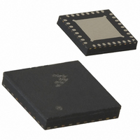
MC13202FC Freescale Semiconductor, MC13202FC Datasheet - Page 24

MC13202FC
Manufacturer Part Number
MC13202FC
Description
IC TXRX RF 2.4GHZ 32-QFN
Manufacturer
Freescale Semiconductor
Datasheet
1.MC13202FCR2.pdf
(30 pages)
Specifications of MC13202FC
Frequency
2.4GHz
Data Rate - Maximum
250kbps
Modulation Or Protocol
802.15.4
Applications
AMR, HID, HVAC, ISM
Power - Output
-27dBm ~ 3dBm
Sensitivity
-92dBm
Voltage - Supply
2 V ~ 3.4 V
Current - Receiving
37mA
Current - Transmitting
30mA
Data Interface
PCB, Surface Mount
Antenna Connector
PCB, Surface Mount
Operating Temperature
-40°C ~ 85°C
Package / Case
32-QFN
Operating Supply Voltage
2.7 V
Mounting Style
SMD/SMT
Minimum Operating Temperature
- 40 C
Operating Temperature (min)
-40C
Operating Temperature (max)
85C
Operating Temperature Classification
Industrial
Lead Free Status / RoHS Status
Lead free / RoHS Compliant
Memory Size
-
Lead Free Status / Rohs Status
Lead free / RoHS Compliant
Figure 14
noise amplifier (LNA) for greater range. An external antenna switch is used to multiplex the antenna
between receive and transmit. An LNA is in the receive path to add gain for greater receive sensitivity.
Two external baluns are required to convert the single-ended antenna switch signals to the differential
signals required by the radio. Separate RFIN and PAO signals are provided for connection with the baluns.
The CT_bias signal is programmed to provide the external switch control, and the polarity of CT_Bias for
the switch control is selectable. CT_bias has a high voltage of VDDA (nominal 1.8Vdc) and may require
a buffer transistor if the antenna switch requires a higher voltage control signal.
Figure 14
receive side, the RX antenna is ac-coupled to the differential RFIN inputs and these capacitors along with
inductor L1 form a matching network. Inductors L2 and L3 are ac-coupled to ground to form a frequency
trap. For the transmit side, the TX antenna is connected to the differential PAO outputs, and inductors L4
and L5 provide DC-biasing to VDDA but are ac-isolated. CT_Bias is not required or used.
24
shows two dual port configurations. First is a single antenna configuration with an external low
also shows a dual antenna configuration where there is a RX antenna and a TX antenna. For the
Using External Antenna Switch with LNA
A nt
S w
V D D
LN A
B a lun
B a lun
Figure 14. Dual Port RF Configuration Examples
B yp ass
B yp ass
MC13202 Technical Data, Rev. 1.5
V D D A
L1
R F IN _ M (P A O _ M )
R F IN _ P (P A O _P )
M C 1320 2/03
P A O _ P
P A O _ M
(A nt S w C tl)
C T _ B ias
RX Antenna
TX Antenna
L1
Bypass
L2
L4
Using Dual Antenna
VDDA
L3
L5
Bypass
RFIN_P (PAO_P)
RFIN_M (PAO_M)
PAO_P
PAO_M
CT_Bias
Freescale Semiconductor
MC13202/03


