LMX9830SM/NOPB National Semiconductor, LMX9830SM/NOPB Datasheet - Page 13
LMX9830SM/NOPB
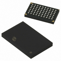
Manufacturer Part Number
LMX9830SM/NOPB
Description
IC SRL PORT MOD BLUETOOTH 60FBGA
Manufacturer
National Semiconductor
Datasheet
1.LMX9830SMNOPB.pdf
(46 pages)
Specifications of LMX9830SM/NOPB
Frequency
2.4GHz
Data Rate - Maximum
704kbps
Modulation Or Protocol
Bluetooth v2.0, Class 2
Applications
PDA's, POS Terminals
Power - Output
0dBm
Sensitivity
-80dBm
Voltage - Supply
2.5 V ~ 3.6 V
Current - Receiving
65mA
Current - Transmitting
65mA
Data Interface
PCB, Surface Mount
Antenna Connector
PCB, Surface Mount
Operating Temperature
-40°C ~ 125°C
Package / Case
60-FBGA
Physical Interfaces
UART
Data Rate
704Kbps
Operating Temperature Range
-40°C To +125°C
Msl
MSL 4 - 72 Hours
Supply Voltage Range
1.6V To 3.6V
Frequency Max
2480MHz
Termination Type
SMD
Rohs Compliant
Yes
Filter Terminals
SMD
Frequency Min
2402MHz
Lead Free Status / RoHS Status
Lead free / RoHS Compliant
Memory Size
-
Lead Free Status / Rohs Status
Compliant
Other names
*LMX9830SM
*LMX9830SM/NOPB
LMX9830SM
*LMX9830SM/NOPB
LMX9830SM


OP4/PG4
PG6
PG7
t
t
PTORRA
PTORBB
In alternate function the pins have pre-defined indication func-
tionality. Please see Table 13 for a description on the alter-
nate indication functionality.
9.5 SYSTEM POWER UP
In order to correctly power-up the LMX9830 the following se-
quence is recommended to be performed:
Apply VCC_IO and V
The RESET_RA# should be driven high. Then RESET_BB#
should be driven high at a recommended time of 1ms after
Note 28: Rise time on power must switch on fast, rise time <500us.
Note 29: Recommended value.
Symbol
Power to Reset _RA#
Reset_RA# to Reset_BB#
Pin
CC
Parameter
to the LMX9830.
Operation Mode pin to configure Transport Layer settings during boot-up
GPIO
RF Traffic indication
TABLE 13. Alternate GPIO Pin Configuration
FIGURE 1. LMX9830 Power on Reset Timing
TABLE 14. LMX9830 Power to Reset timing
V
level to valid reset
V
level to valid reset
CC
CC
and VCC_IO at operating voltage
and VCC_IO at operating voltage
Condition
13
the LMX9830 voltage rails are high. The LMX9830 is properly
reset.
Please see timing diagram, Figure 1.
ESR of the crystal also has impact on the startup time of the
crystal oscillator circuit of the LMX9830 (See Table 14 and
Table 15).
Description
(Note 28)
(Note 29)
<500
Min
1
Typ
Max
www.national.com
20180009
Unit
ms
µs
Related parts for LMX9830SM/NOPB
Image
Part Number
Description
Manufacturer
Datasheet
Request
R

Part Number:
Description:
Manufacturer:
National Semiconductor
Datasheet:

Part Number:
Description:
National Semiconductor [8-Bit D/A Converter]
Manufacturer:
National Semiconductor
Datasheet:
Part Number:
Description:
National Semiconductor [Media Coprocessor]
Manufacturer:
National Semiconductor
Datasheet:
Part Number:
Description:
Digitally Controlled Tone and Volume Circuit with Stereo Audio Power Amplifier, Microphone Preamp Stage and National 3D Sound
Manufacturer:
National Semiconductor
Datasheet:
Part Number:
Description:
Digitally Controlled Tone and Volume Circuit with Stereo Audio Power Amplifier, Microphone Preamp Stage and National 3D Sound
Manufacturer:
National Semiconductor
Datasheet:
Part Number:
Description:
AC97 Rev 2 Codec with Sample Rate Conversion and National 3D Sound
Manufacturer:
National Semiconductor
Part Number:
Description:
Manufacturer:
National Semiconductor
Datasheet:
Part Number:
Description:
Manufacturer:
National Semiconductor
Datasheet:
Part Number:
Description:
General Purpose, Low Voltage, Low Power, Rail-to-Rail Output Operational Amplifiers
Manufacturer:
National Semiconductor
Datasheet:
Part Number:
Description:
8-bit 20 MSPS flash A/D converter.
Manufacturer:
National Semiconductor
Datasheet:
Part Number:
Description:
Low Noise Quad Operational Amplifier
Manufacturer:
National Semiconductor
Datasheet:
Part Number:
Description:
Quad Differential Line Receivers
Manufacturer:
National Semiconductor
Datasheet:
Part Number:
Description:
Quad High Speed Trapezoidal? Bus Transceiver
Manufacturer:
National Semiconductor
Datasheet:
Part Number:
Description:
Dual Line Receiver
Manufacturer:
National Semiconductor
Datasheet: