LMX9830SM/NOPB National Semiconductor, LMX9830SM/NOPB Datasheet - Page 39
LMX9830SM/NOPB
Manufacturer Part Number
LMX9830SM/NOPB
Description
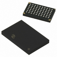
IC SRL PORT MOD BLUETOOTH 60FBGA
Manufacturer
National Semiconductor
Datasheet
1.LMX9830SMNOPB.pdf
(46 pages)
Specifications of LMX9830SM/NOPB
Frequency
2.4GHz
Data Rate - Maximum
704kbps
Modulation Or Protocol
Bluetooth v2.0, Class 2
Applications
PDA's, POS Terminals
Power - Output
0dBm
Sensitivity
-80dBm
Voltage - Supply
2.5 V ~ 3.6 V
Current - Receiving
65mA
Current - Transmitting
65mA
Data Interface
PCB, Surface Mount
Antenna Connector
PCB, Surface Mount
Operating Temperature
-40°C ~ 125°C
Package / Case
60-FBGA
Physical Interfaces
UART
Data Rate
704Kbps
Operating Temperature Range
-40°C To +125°C
Msl
MSL 4 - 72 Hours
Supply Voltage Range
1.6V To 3.6V
Frequency Max
2480MHz
Termination Type
SMD
Rohs Compliant
Yes
Filter Terminals
SMD
Frequency Min
2402MHz
Lead Free Status / RoHS Status
Lead free / RoHS Compliant
Memory Size
-
Lead Free Status / Rohs Status
Compliant
Other names
*LMX9830SM
*LMX9830SM/NOPB
LMX9830SM
*LMX9830SM/NOPB
LMX9830SM


15.0 Application Information
Figure 19 represents a typical system functional schematic
for the LMX9830 in its normal 3.0V or 3.3V system interface
operation.
In Figure 20 represents a typical system functional schematic
for the LMX9830 in its 1.8V system interface operation.
15.1 ANTENNA MATCHING NETWORK
The antenna matching network may or may not be required,
depending upon the impedance of the antenna chosen and
the trace impedance on the PCB. A 6.8 pF blocking capacitor
is recommended.
Note: Additional L network placement is recommended for tuning the trace
15.2 FILTERED POWER SUPPLY
It is important to provide the LMX9830 with adequate ground
planes and a filtered power supply. It is highly recommended
that a 0.1 µF and a 10 pF bypass capacitor be placed as close
as possible to V
operations.
Note: For 1.8V operations V
15.3 HOST INTERFACE
To set the logic thresholds of the LMX9830 to match the host
system, IOVCC (pin C4) must be connected to the logic power
impedance if needed.
tied directly to ground.
CC
(pin E1) on the LMX9830 for 2.5V and 3.3V
CC
filtering is not required and V
CC
should be
39
supply of the host system. It is highly recommended that a 10
pF bypass capacitor be placed as close as possible to the
IOVCC pad on the LMX9830.
15.4 FREQUENCY AND BAUD RATE SELECTIONS
OP3, OP4, OP5 can be strapped to the host logic 0 and 1
levels to set the host interface boot-up configuration. Alterna-
tively all OP3, OP4, OP5 can be hardwired over 1kW pullup/
pulldown resistors. See Table 18.
15.5 START UP SEQUENCE OPTIONS
OP6, OP7, and Env1 can be left unconnected (both OP6 and
OP7 are pulled low and ENV1 is pulled high internally), These
can be hardwired over 1kW pullup/pulldown resistors. See
Table 17.
15.6 CLOCK INPUT
The clock source must be placed as close as possible to the
LMX9830. The quality of the radio performance is directly re-
lated to the quality of the clock source connected to the
oscillator port on the LMX9830. Careful attention must be paid
to the crystal/oscillator parameters or radio performance
could be drastically reduced.
15.7 SCHEMATIC AND LAYOUT EXAMPLES
See Figure 19, Figure 20, and full schematic in Section 16.0
Reference Design.
www.national.com
Related parts for LMX9830SM/NOPB
Image
Part Number
Description
Manufacturer
Datasheet
Request
R

Part Number:
Description:
Manufacturer:
National Semiconductor
Datasheet:

Part Number:
Description:
National Semiconductor [8-Bit D/A Converter]
Manufacturer:
National Semiconductor
Datasheet:
Part Number:
Description:
National Semiconductor [Media Coprocessor]
Manufacturer:
National Semiconductor
Datasheet:
Part Number:
Description:
Digitally Controlled Tone and Volume Circuit with Stereo Audio Power Amplifier, Microphone Preamp Stage and National 3D Sound
Manufacturer:
National Semiconductor
Datasheet:
Part Number:
Description:
Digitally Controlled Tone and Volume Circuit with Stereo Audio Power Amplifier, Microphone Preamp Stage and National 3D Sound
Manufacturer:
National Semiconductor
Datasheet:
Part Number:
Description:
AC97 Rev 2 Codec with Sample Rate Conversion and National 3D Sound
Manufacturer:
National Semiconductor
Part Number:
Description:
Manufacturer:
National Semiconductor
Datasheet:
Part Number:
Description:
Manufacturer:
National Semiconductor
Datasheet:
Part Number:
Description:
General Purpose, Low Voltage, Low Power, Rail-to-Rail Output Operational Amplifiers
Manufacturer:
National Semiconductor
Datasheet:
Part Number:
Description:
8-bit 20 MSPS flash A/D converter.
Manufacturer:
National Semiconductor
Datasheet:
Part Number:
Description:
Low Noise Quad Operational Amplifier
Manufacturer:
National Semiconductor
Datasheet:
Part Number:
Description:
Quad Differential Line Receivers
Manufacturer:
National Semiconductor
Datasheet:
Part Number:
Description:
Quad High Speed Trapezoidal? Bus Transceiver
Manufacturer:
National Semiconductor
Datasheet:
Part Number:
Description:
Dual Line Receiver
Manufacturer:
National Semiconductor
Datasheet: