SX1212IWLTRT Semtech, SX1212IWLTRT Datasheet - Page 3
SX1212IWLTRT
Manufacturer Part Number
SX1212IWLTRT
Description
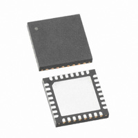
IC TXRX 300MHZ-510MHZ 32-TQFN
Manufacturer
Semtech
Datasheet
1.SX1212IWLTRT.pdf
(77 pages)
Specifications of SX1212IWLTRT
Frequency
300MHz ~ 510MHz
Data Rate - Maximum
150kbps
Modulation Or Protocol
FSK, OOK
Applications
AMR, ISM, Home Automation, Process Control
Power - Output
12.5dBm
Sensitivity
-110dBm
Voltage - Supply
2.1 V ~ 3.6 V
Current - Receiving
3mA
Current - Transmitting
25mA
Data Interface
PCB, Surface Mount
Antenna Connector
PCB, Surface Mount
Operating Temperature
-40°C ~ 85°C
Package / Case
32-TQFN
Operating Temperature (min)
-40C
Operating Temperature (max)
85C
Operating Temperature Classification
Industrial
Modulation Type
FSK/OOK
Package Type
TQFN EP
Operating Supply Voltage (min)
2.1V
Operating Supply Voltage (typ)
2.5/3.3V
Operating Supply Voltage (max)
3.6V
Lead Free Status / RoHS Status
Lead free / RoHS Compliant
Memory Size
-
Lead Free Status / Rohs Status
Supplier Unconfirmed
Other names
SX1212IWLTR
Available stocks
Company
Part Number
Manufacturer
Quantity
Price

Part Number:
SX1212IWLTRT
Manufacturer:
SEMTECH/美国升特
Quantity:
20 000


Index of Figures
Figure 1: SX1212 Simplified Block Diagram .................................. 5
Figure 2: SX1212 Pin Diagram ...................................................... 6
Figure 3: SX1212 Detailed Block Diagram .................................. 12
Figure 4: Power Supply Breakdown............................................. 13
Figure 5: Frequency Synthesizer Description .............................. 14
Figure 6: LO Generator ................................................................ 14
Figure 7: Loop Filter ..................................................................... 16
Figure 8: Transmitter Architecture ............................................... 18
Figure 9: I(t), Q(t) Overview ......................................................... 18
Figure 10: PA Control................................................................... 21
Figure 11: Optimal Load Impedance Chart .................................. 21
Figure 13: Front-end Description ................................................. 22
Figure 14: Receiver Architecture ................................................. 23
Figure 15: FSK Receiver Setting ................................................. 23
Figure 16: OOK Receiver Setting ................................................ 23
Figure 17: Active Channel Filter Description................................ 24
Figure 18: Butterworth Filter's Actual BW .................................... 26
Figure 19: Polyphase Filter's Actual BW...................................... 26
Figure 20: RSSI Dynamic Range ................................................. 27
Figure 21: RSSI IRQ Timings ...................................................... 28
Figure 22: OOK Demodulator Description ................................... 29
Figure 23: Floor Threshold Optimization...................................... 30
Figure 24: BitSync Description..................................................... 31
Figure 25: SX1212’s Data Processing Conceptual View ............. 34
Figure 26: SPI Interface Overview and uC Connections ............. 35
Figure 27: Write Register Sequence ............................................ 36
Figure 28: Read Register Sequence............................................ 37
Figure 29: Write Bytes Sequence (ex: 2 bytes) ........................... 37
Figure 30: Read Bytes Sequence (ex: 2 bytes) ........................... 38
Figure 31: FIFO and Shift Register (SR)...................................... 38
Figure 32: FIFO Threshold IRQ Source Behavior........................ 39
Rev 2 – June 18th, 2009
Figure 12: Recommended PA Biasing and Output Matching ..... 22
ADVANCED COMMUNICATIONS & SENSING
Page 3 of 77
Figure 33: Sync Word Recognition ...............................................40
Figure 34: Continuous Mode Conceptual View.............................41
Figure 35: Tx Processing in Continuous Mode .............................41
Figure 36: Rx Processing in Continuous Mode.............................42
Figure 37: uC Connections in Continuous Mode ..........................43
Figure 38: Buffered Mode Conceptual View .................................44
Figure 39: Tx processing in Buffered Mode (FIFO size = 16,
Figure 40: Rx Processing in Buffered Mode (FIFO size=16,
Figure 41: uC Connections in Buffered Mode...............................47
Figure 42: Packet Mode Conceptual View....................................49
Figure 43: Fixed Length Packet Format........................................50
Figure 44: Variable Length Packet Format ...................................51
Figure 45: CRC Implementation ...................................................53
Figure 46: Manchester Encoding/Decoding..................................54
Figure 47: Data Whitening ............................................................54
Figure 48: uC Connections in Packet Mode .................................55
Figure 49: Optimized Rx Cycle .....................................................67
Figure 50: Optimized Tx Cycle......................................................68
Figure 51: Tx Hop Cycle ...............................................................69
Figure 52: Rx Hop Cycle ...............................................................70
Figure 53: Rx
Figure 54: POR Timing Diagram...................................................72
Figure 55: Manual Reset Timing Diagram ....................................72
Figure 56: Reference Design Circuit Schematic ...........................73
Figure 57: Reference Design‘s Stackup .......................................74
Figure 58: Reference Design Layout (top view)............................74
Figure 59: Package Outline Drawing ............................................75
Figure 60: PCB Land Pattern ........................................................75
Figure 61: Tape & Reel Dimensions .............................................76
Tx_start_irq_0=0) ...............................................................45
Fifo_fill_method=0).............................................................46
Tx
Rx Cycle ...................................................71
www.semtech.com
SX1212
Related parts for SX1212IWLTRT
Image
Part Number
Description
Manufacturer
Datasheet
Request
R

Part Number:
Description:
EVALUATION BOARD
Manufacturer:
Semtech
Datasheet:
Part Number:
Description:
EVALUATION BOARD
Manufacturer:
Semtech
Datasheet:
Part Number:
Description:
VOLTAGE SUPPRESSOR, TRANSIENT SEMTECH
Manufacturer:
Semtech
Datasheet:

Part Number:
Description:
HIGH VOLTAGE CAPACITORS MONOLITHIC CERAMIC TYPE
Manufacturer:
Semtech Corporation
Datasheet:
Part Number:
Description:
EZ1084CM5.0 AMP POSITIVE VOLTAGE REGULATOR
Manufacturer:
Semtech Corporation
Datasheet:
Part Number:
Description:
3.0 AMP LOW DROPOUT POSITIVE VOLTAGE REGULATORS
Manufacturer:
Semtech Corporation
Datasheet:
Part Number:
Description:
Manufacturer:
Semtech Corporation
Datasheet:
Part Number:
Description:
RailClamp Low Capacitance TVS Diode Array
Manufacturer:
Semtech Corporation
Datasheet:
Part Number:
Description:
Manufacturer:
Semtech Corporation
Datasheet:
Part Number:
Description:
Manufacturer:
Semtech Corporation
Datasheet:
Part Number:
Description:
Manufacturer:
Semtech Corporation
Datasheet:
Part Number:
Description:
Manufacturer:
Semtech Corporation
Datasheet: