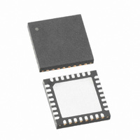
SX1212IWLTRT Semtech, SX1212IWLTRT Datasheet - Page 43

SX1212IWLTRT
Manufacturer Part Number
SX1212IWLTRT
Description
IC TXRX 300MHZ-510MHZ 32-TQFN
Manufacturer
Semtech
Datasheet
1.SX1212IWLTRT.pdf
(77 pages)
Specifications of SX1212IWLTRT
Frequency
300MHz ~ 510MHz
Data Rate - Maximum
150kbps
Modulation Or Protocol
FSK, OOK
Applications
AMR, ISM, Home Automation, Process Control
Power - Output
12.5dBm
Sensitivity
-110dBm
Voltage - Supply
2.1 V ~ 3.6 V
Current - Receiving
3mA
Current - Transmitting
25mA
Data Interface
PCB, Surface Mount
Antenna Connector
PCB, Surface Mount
Operating Temperature
-40°C ~ 85°C
Package / Case
32-TQFN
Operating Temperature (min)
-40C
Operating Temperature (max)
85C
Operating Temperature Classification
Industrial
Modulation Type
FSK/OOK
Package Type
TQFN EP
Operating Supply Voltage (min)
2.1V
Operating Supply Voltage (typ)
2.5/3.3V
Operating Supply Voltage (max)
3.6V
Lead Free Status / RoHS Status
Lead free / RoHS Compliant
Memory Size
-
Lead Free Status / Rohs Status
Supplier Unconfirmed
Other names
SX1212IWLTR
Available stocks
Company
Part Number
Manufacturer
Quantity
Price
Part Number:
SX1212IWLTRT
Manufacturer:
SEMTECH/美国升特
Quantity:
20 000
Note that some connections may not be needed depending on the application:
In addition, NSS_DATA pin (unused in continuous mode) should be pulled-up to VDD through a 100 kΩ resistor.
Please refer to Table 13 for SX1212’s pins configuration
Table 19: Relevant Configuration Registers in Continuous Mode (data processing related only)
Tx Mode:
Rx Mode:
Rev 2 – June 18th, 2009
ADVANCED COMMUNICATIONS & SENSING
SYNCParam
IRQParam
MCParam
RXParam
IRQ_0: if Sync and RSSI interrupts are not used. In this case, leave floating.
IRQ_1: if the chip is never used in Tx FSK mode (DCLK connection is not compulsory in Rx and Tx OOK
modes). In this case, leave floating.
MISO: if no read register access is needed. In this case, pull-up to VDD through a 100 kΩ resistor.
Configure all data processing related registers listed below appropriately. In this example we assume that both
Bit synchronizer and Sync word recognition are on.
Go to Tx mode (and wait for Tx to be ready, see Figure 50)
Send all packet’s bits on DATA pin synchronously with DCLK signal provided on IRQ_1
Go to Sleep mode
Program Rx interrupts: IRQ_0 mapped to Sync (Rx_stby_irq_0=”00”) and IRQ_1 mapped to DCLK (Bit
synchronizer enabled)
Go to Rx mode (note that Rx is not ready immediately, see Figure 49)
Wait for Sync interrupt
Get all packet bits on DATA pin synchronously with DCLK signal provided on IRQ_1
Go to Sleep mode
5.3.5. uC Connections
5.3.6. Continuous Mode Example
Rx_stby_irq_0
Data_mode_x
Sync_value
Sync_size
Sync_on
Sync_tol
Figure 37: uC Connections in Continuous Mode
SX1212
Tx
X
IRQ_1 (DCLK)
NSS_CONFIG
IRQ_0
DATA
MOSI
MISO
SCK
Rx
X
X
X
X
X
X
Page 43 of 77
Description
Defines data operation mode (
Defines IRQ_0 source in Rx mode
Enables Sync word recognition
Defines Sync word size
Defines the error tolerance on Sync word recognition
Defines Sync word value
uC
Continuous)
www.semtech.com
SX1212


