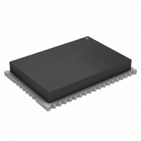
ATZB-24-A2 Atmel, ATZB-24-A2 Datasheet - Page 9

ATZB-24-A2
Manufacturer Part Number
ATZB-24-A2
Description
KIT MOD 802.15.4/ZIGB 2.4GHZ ANT
Manufacturer
Atmel
Specifications of ATZB-24-A2
Frequency
2.4GHz
Data Rate - Maximum
250kbps
Modulation Or Protocol
802.15.4 Zigbee
Applications
Home/Building Automation, Industrial Control and Monitoring
Power - Output
3dBm
Sensitivity
-101dBm
Voltage - Supply
1.8 V ~ 3.6 V
Current - Receiving
19mA
Current - Transmitting
18mA
Data Interface
PCB, Surface Mount
Memory Size
128kBytes Flash, 8kBytes RAM, 4kBytes EEPROM
Antenna Connector
On-Board, Chip
Operating Temperature
-40°C ~ 85°C
Package / Case
Module
Tool Type
Wireless Development Kit
Core Architecture
AVR
Cpu Core
AVR 8
Data Bus Width
8 bit
Description/function
ZigBit 2.4 GHz Dual Chip Antenna
Wireless Frequency
2.4 GHz
Interface Type
UART, I2C, SPI
Operating Voltage
1.8 V to 3.6 V
Output Power
3 dBm
Antenna
Chip Antenna
Operating Temperature Range
- 40 C to + 85 C
Lead Free Status / RoHS Status
Lead free / RoHS Compliant
Available stocks
Company
Part Number
Manufacturer
Quantity
Price
Part Number:
ATZB-24-A2
Manufacturer:
ATMEL/爱特梅尔
Quantity:
20 000
Company:
Part Number:
ATZB-24-A2R
Manufacturer:
CIRRUS
Quantity:
201
6.3
6.4
6.5
8069Q–AVR–12/10
Register File
ALU - Arithmetic Logic Unit
Program Flow
concept enables instructions to be executed in every clock cycle. The program memory is In-
System Re-programmable Flash memory.
The fast-access Register File contains 32 x 8-bit general purpose working registers with single
clock cycle access time. This allows single-cycle Arithmetic Logic Unit (ALU) operation. In a typ-
ical ALU cycle, the operation is performed on two Register File operands, and the result is stored
back in the Register File.
Six of the 32 registers can be used as three 16-bit address register pointers for data space
addressing - enabling efficient address calculations. One of these address pointers can also be
used as an address pointer for look up tables in Flash program memory.
The high performance Arithmetic Logic Unit (ALU) supports arithmetic and logic operations
between registers or between a constant and a register. Single register operations can also be
executed. Within a single clock cycle, arithmetic operations between general purpose registers
or between a register and an immediate are executed. After an arithmetic or logic operation, the
Status Register is updated to reflect information about the result of the operation.
The ALU operations are divided into three main categories – arithmetic, logical, and bit-func-
tions. Both 8- and 16-bit arithmetic is supported, and the instruction set allows for efficient
implementation of 32-bit arithmetic. The ALU also provides a powerful multiplier supporting both
signed and unsigned multiplication and fractional format.
When the device is powered on, the CPU starts to execute instructions from the lowest address
in the Flash Program Memory ‘0’. The Program Counter (PC) addresses the next instruction to
be fetched. After a reset, the PC is set to location ‘0’.
Program flow is provided by conditional and unconditional jump and call instructions, capable of
addressing the whole address space directly. Most AVR instructions use a 16-bit word format,
while a limited number uses a 32-bit format.
During interrupts and subroutine calls, the return address PC is stored on the Stack. The Stack
is effectively allocated in the general data SRAM, and consequently the Stack size is only limited
by the total SRAM size and the usage of the SRAM. After reset the Stack Pointer (SP) points to
the highest address in the internal SRAM. The SP is read/write accessible in the I/O memory
space, enabling easy implementation of multiple stacks or stack areas. The data SRAM can
easily be accessed through the five different addressing modes supported in the AVR CPU.
XMEGA A4
9


