CPV362M4F Vishay, CPV362M4F Datasheet - Page 2
CPV362M4F
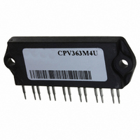
Manufacturer Part Number
CPV362M4F
Description
IGBT SIP MODULE 600V 8.8A IMS-2
Manufacturer
Vishay
Datasheet
1.CPV362M4F.pdf
(10 pages)
Specifications of CPV362M4F
Configuration
Three Phase Inverter
Voltage - Collector Emitter Breakdown (max)
600V
Vce(on) (max) @ Vge, Ic
1.66V @ 15V, 8.8A
Current - Collector (ic) (max)
8.8A
Current - Collector Cutoff (max)
250µA
Input Capacitance (cies) @ Vce
0.34nF @ 30V
Power - Max
23W
Input
Standard
Ntc Thermistor
No
Mounting Type
Through Hole
Package / Case
19-SIP (13 Leads), IMS-2
Lead Free Status / RoHS Status
Contains lead / RoHS non-compliant
Igbt Type
-
Other names
*CPV362M4F
VS-CPV362M4F
VS-CPV362M4F
VSCPV362M4F
VSCPV362M4F
VS-CPV362M4F
VS-CPV362M4F
VSCPV362M4F
VSCPV362M4F
Available stocks
Company
Part Number
Manufacturer
Quantity
Price

Company:
Part Number:
CPV362M4F
Manufacturer:
PRX
Quantity:
530


CPV362M4F
Electrical Characteristics @ T
Switching Characteristics @ T
Notes:
E
V
V
V
g
I
V
I
Q
Q
Q
t
t
t
t
E
E
t
t
t
t
E
C
C
C
t
I
Q
di
CES
GES
d(on)
d(off)
f
d(on)
d(off)
f
rr
r
r
rr
ts
fe
V
on
off
ts
oes
(BR)CES
CE(on)
GE(th)
g
ge
ies
res
FM
gc
V
rr
(rec)M
(BR)CES
GE(th)
limited by max. junction temperature.
( See fig. 20 )
Repetitive rating; V
/dt
/ T
/ T
J
J
Collector-to-Emitter Breakdown Voltage
Temperature Coeff. of Breakdown Voltage
Collector-to-Emitter Saturation Voltage
Gate Threshold Voltage
Temperature Coeff. of Threshold Voltage
Forward Transconductance
Zero Gate Voltage Collector Current
Diode Forward Voltage Drop
Gate-to-Emitter Leakage Current
Total Gate Charge (turn-on)
Gate - Emitter Charge (turn-on)
Gate - Collector Charge (turn-on)
Turn-On Delay Time
Rise Time
Turn-Off Delay Time
Fall Time
Turn-On Switching Loss
Turn-Off Switching Loss
Total Switching Loss
Turn-On Delay Time
Rise Time
Turn-Off Delay Time
Fall Time
Total Switching Loss
Input Capacitance
Output Capacitance
Reverse Transfer Capacitance
Diode Reverse Recovery Time
Diode Peak Reverse Recovery Current
Diode Reverse Recovery Charge
Diode Peak Rate of Fall of Recovery
During t
b
Parameter
Parameter
GE
=20V, pulse width
J
J
= 25°C (unless otherwise specified)
= 25°C (unless otherwise specified)
V
Pulse width
R
CC
G
= 50 , ( See fig. 19 )
Min. Typ. Max. Units
Min. Typ. Max. Units
=80%(V
600
––– 0.72 –––
––– 1.66 –––
––– 1.42 –––
–––
–––
–––
–––
–––
–––
–––
–––
–––
–––
–––
–––
––– 0.23 –––
––– 0.33 –––
––– 0.45 0.70
–––
–––
–––
–––
––– 0.93 –––
–––
–––
–––
–––
–––
–––
–––
–––
–––
–––
–––
––– 1.41
–––
3.0
2.9
–––
––– 1700
––– ±100
200
435
124
240
210
–––
-11
–––
214
364
340
1.4
5.9
3.5
5.0
1.3
4.0
4.5
30
13
49
22
48
25
63
37
55
65
CES
80µs; duty factor
), V
–––
–––
––– mV/°C V
–––
250
–––
–––
300
320
–––
–––
–––
–––
–––
–––
138
360
–––
–––
1.7
6.0
1.7
1.6
6.0
8.0
45
20
55
90
50
GE
=20V, L=10µH,
V/°C
A/µs
nA
µA
nC
mJ
mJ
nC
V
V
V
ns
ns
pF
ns
S
A
ƒ = 1.0MHz
V
V
I
I
I
V
V
V
V
I
I
V
I
V
See Fig. 8
T
I
V
Energy losses include "tail" and
diode reverse recovery
See Fig. 9, 10, 18
T
I
V
Energy losses include "tail" and
diode reverse recovery
V
V
T
T
T
T
T
T
T
T
C
C
C
C
C
C
C
C
J
J
J
GE
GE
CE
CE
CE
GE
GE
GE
CC
J
GE
J
GE
GE
CC
J
J
J
J
J
= 4.8A, T
= 8.0A, T
= 4.8A
= 8.8A
= 8.0A
= 4.8A
= 4.8A, V
= 4.8A, V
= 25°C
= 125°C
= 125°C
= 125°C
= 150°C,
= 25°C
= 25°C
= 25°C
= 25°C
= 125°C
0.1%.
= V
= V
= 100V, I
= 0V, I
= 0V, I
= 0V, V
= 0V, V
= 15V, R
= 15V, R
= ±20V
= 400V
= 0V
= 30V
GE
GE
shot.
, I
, I
C
C
J
J
CE
CC
CC
C
C
CE
See Fig.
See Fig.
See Fig.
See Fig.
Pulse width 5.0µs, single
= 150°C
= 150°C
= 1.0mA
= 250µA
G
G
Conditions
Conditions
C
= 250µA
= 250µA
= 600V, T
= 480V
= 50
= 480V
= 50
= 600V
= 4.8A
17
See Fig. 10,11, 18
14
15
16
See Fig. 7
di/dt = 200A/µs
See Fig. 2, 5
V
See Fig. 13
J
GE
= 150°C
I
V
F
R
= 15V
= 8.0A
= 200V
Related parts for CPV362M4F
Image
Part Number
Description
Manufacturer
Datasheet
Request
R

Part Number:
Description:
357-036-542-201 CARDEDGE 36POS DL .156 BLK LOPRO
Manufacturer:
Vishay
Datasheet:
Part Number:
Description:
357-036-542-201 CARDEDGE 36POS DL .156 BLK LOPRO
Manufacturer:
Vishay
Datasheet:
Part Number:
Description:
357-036-542-201 CARDEDGE 36POS DL .156 BLK LOPRO
Manufacturer:
Vishay
Datasheet:
Part Number:
Description:
357-036-542-201 CARDEDGE 36POS DL .156 BLK LOPRO
Manufacturer:
Vishay
Datasheet:
Part Number:
Description:
357-036-542-201 CARDEDGE 36POS DL .156 BLK LOPRO
Manufacturer:
Vishay
Datasheet:
Part Number:
Description:
357-036-542-201 CARDEDGE 36POS DL .156 BLK LOPRO
Manufacturer:
Vishay
Datasheet:
Part Number:
Description:
357-036-542-201 CARDEDGE 36POS DL .156 BLK LOPRO
Manufacturer:
Vishay
Datasheet:
Part Number:
Description:
357-036-542-201 CARDEDGE 36POS DL .156 BLK LOPRO
Manufacturer:
Vishay
Datasheet:
Part Number:
Description:
357-036-542-201 CARDEDGE 36POS DL .156 BLK LOPRO
Manufacturer:
Vishay
Datasheet:
Part Number:
Description:
357-036-542-201 CARDEDGE 36POS DL .156 BLK LOPRO
Manufacturer:
Vishay
Datasheet:
Part Number:
Description:
357-036-542-201 CARDEDGE 36POS DL .156 BLK LOPRO
Manufacturer:
Vishay
Datasheet:
Part Number:
Description:
357-036-542-201 CARDEDGE 36POS DL .156 BLK LOPRO
Manufacturer:
Vishay
Datasheet:
Part Number:
Description:
357-036-542-201 CARDEDGE 36POS DL .156 BLK LOPRO
Manufacturer:
Vishay
Datasheet:
Part Number:
Description:
357-036-542-201 CARDEDGE 36POS DL .156 BLK LOPRO
Manufacturer:
Vishay
Datasheet:
Part Number:
Description:
357-036-542-201 CARDEDGE 36POS DL .156 BLK LOPRO
Manufacturer:
Vishay
Datasheet: