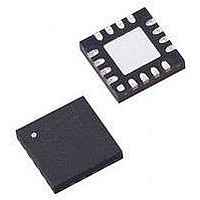
PIC16F1824-I/ML Microchip Technology, PIC16F1824-I/ML Datasheet - Page 75

PIC16F1824-I/ML
Manufacturer Part Number
PIC16F1824-I/ML
Description
IC PIC MCU 8BIT 14KB FLSH 16QFN
Manufacturer
Microchip Technology
Series
PIC® XLP™ 16Fr
Datasheets
1.PIC16F722-ISS.pdf
(8 pages)
2.PIC16F1826-IP.pdf
(40 pages)
3.PIC16F1824-ISL.pdf
(2 pages)
4.PIC16F1824-ISL.pdf
(419 pages)
5.PIC16F1824-ISL.pdf
(10 pages)
Specifications of PIC16F1824-I/ML
Core Size
8-Bit
Program Memory Size
7KB (4K x 14)
Core Processor
PIC
Speed
32MHz
Connectivity
I²C, SPI, UART/USART
Peripherals
Brown-out Detect/Reset, POR, PWM, WDT
Number Of I /o
11
Program Memory Type
FLASH
Eeprom Size
256 x 8
Ram Size
256 x 8
Voltage - Supply (vcc/vdd)
1.8 V ~ 5.5 V
Data Converters
A/D 8x10b
Oscillator Type
Internal
Operating Temperature
-40°C ~ 85°C
Package / Case
16-VQFN Exposed Pad
Controller Family/series
PIC16F
No. Of I/o's
12
Eeprom Memory Size
256Byte
Ram Memory Size
256Byte
Cpu Speed
32MHz
No. Of Timers
5
Lead Free Status / RoHS Status
Lead free / RoHS Compliant
Available stocks
Company
Part Number
Manufacturer
Quantity
Price
Company:
Part Number:
PIC16F1824-I/ML
Manufacturer:
KEMET
Quantity:
1 000
Part Number:
PIC16F1824-I/ML
Manufacturer:
MICROCHIP/微芯
Quantity:
20 000
- PIC16F722-ISS PDF datasheet
- PIC16F1826-IP PDF datasheet #2
- PIC16F1824-ISL PDF datasheet #3
- PIC16F1824-ISL PDF datasheet #4
- PIC16F1824-ISL PDF datasheet #5
- Current page: 75 of 419
- Download datasheet (4Mb)
6.0
The reference clock module provides the ability to send
a divided clock to the clock output pin of the device
(CLKR) and provide a secondary internal clock source
to the modulator module. This module is available in all
oscillator configurations and allows the user to select a
greater range of clock submultiples to drive external
devices in the application. The reference clock module
includes the following features:
• System clock is the source
• Available in all oscillator configurations
• Programmable clock divider
• Output enable to a port pin
• Selectable duty cycle
• Slew rate control
The reference clock module is controlled by the CLKR-
CON register
ting the CLKREN bit. To output the divided clock signal
to the CLKR port pin, the CLKROE bit must be set. The
CLKRDIV<2:0> bits enable the selection of 8 different
clock divider options. The CLKRDC<1:0> bits can be
used to modify the duty cycle of the output clock
CLKRSLR bit controls slew rate limiting.
For information on using the reference clock output
with the modulator module, see
Signal
6.1
The slew rate limitation on the output port pin can be
disabled. The Slew Rate limitation can be removed by
clearing the CLKRSLR bit in the CLKRCON register.
6.2
Upon any device Reset, the reference clock module is
disabled. The user’s firmware is responsible for
initializing the module before enabling the output. The
registers are reset to their default values.
2010 Microchip Technology Inc.
Note 1: If the base clock rate is selected without
Modulator”.
REFERENCE CLOCK MODULE
Slew Rate
Effects of a Reset
a divider, the output clock will always
have a duty cycle equal to that of the
source clock, unless a 0% duty cycle is
selected. If the clock divider is set to base
clock/2, then 25% and 75% duty cycle
accuracy will be dependent upon the
source clock.
(Register
6-1) and is enabled when set-
Section 23.0 “Data
(1)
. The
Preliminary
6.3
There are two cases when the reference clock output
signal cannot be output to the CLKR pin, if:
• LP, XT, or HS oscillator mode is selected.
• CLKOUT function is enabled.
Even if either of these cases are true, the module can
still be enabled and the reference clock signal may be
used in conjunction with the modulator module.
6.3.1
If LP, XT, or HS oscillator modes are selected, the
OSC2/CLKR pin must be used as an oscillator input pin
and the CLKR output cannot be enabled. See
Section 5.2 “Clock Source Types”
tion on different oscillator modes.
6.3.2
The CLKOUT function has a higher priority than the ref-
erence clock module. Therefore, if the CLKOUT func-
tion is enabled by the CLKOUTEN bit in Configuration
Word 1, F
Reference
more information.
6.4
As the reference clock module relies on the system
clock as its source, and the system clock is disabled in
Sleep, the module does not function in Sleep, even if
an external clock source or the Timer1 clock source is
configured as the system clock. The module outputs
will remain in their current state until the device exits
Sleep.
PIC16(L)F1824/1828
Conflicts with the CLKR pin
Operation During Sleep
OSC
Section 4.0 “Device Configuration”
OSCILLATOR MODES
CLKOUT FUNCTION
/4 will always be output on the port pin.
DS41419B-page 75
for more informa-
for
Related parts for PIC16F1824-I/ML
Image
Part Number
Description
Manufacturer
Datasheet
Request
R

Part Number:
Description:
IC, 8BIT MCU, PIC16F, 32MHZ, SOIC-18
Manufacturer:
Microchip Technology
Datasheet:

Part Number:
Description:
IC, 8BIT MCU, PIC16F, 32MHZ, SSOP-20
Manufacturer:
Microchip Technology
Datasheet:

Part Number:
Description:
IC, 8BIT MCU, PIC16F, 32MHZ, DIP-18
Manufacturer:
Microchip Technology
Datasheet:

Part Number:
Description:
IC, 8BIT MCU, PIC16F, 32MHZ, QFN-28
Manufacturer:
Microchip Technology
Datasheet:

Part Number:
Description:
IC, 8BIT MCU, PIC16F, 32MHZ, QFN-28
Manufacturer:
Microchip Technology
Datasheet:

Part Number:
Description:
IC, 8BIT MCU, PIC16F, 32MHZ, QFN-28
Manufacturer:
Microchip Technology
Datasheet:

Part Number:
Description:
IC, 8BIT MCU, PIC16F, 32MHZ, SSOP-20
Manufacturer:
Microchip Technology
Datasheet:

Part Number:
Description:
IC, 8BIT MCU, PIC16F, 20MHZ, DIP-40
Manufacturer:
Microchip Technology
Datasheet:

Part Number:
Description:
IC, 8BIT MCU, PIC16F, 32MHZ, QFN-28
Manufacturer:
Microchip Technology
Datasheet:

Part Number:
Description:
IC, 8BIT MCU, PIC16F, 20MHZ, MQFP-44
Manufacturer:
Microchip Technology
Datasheet:

Part Number:
Description:
IC, 8BIT MCU, PIC16F, 20MHZ, QFN-20
Manufacturer:
Microchip Technology
Datasheet:

Part Number:
Description:
IC, 8BIT MCU, PIC16F, 32MHZ, QFN-28
Manufacturer:
Microchip Technology
Datasheet:

Part Number:
Description:
MCU 14KB FLASH 768B RAM 64-TQFP
Manufacturer:
Microchip Technology
Datasheet:

Part Number:
Description:
7 KB Flash, 384 Bytes RAM, 32 MHz Int. Osc, 16 I/0, Enhanced Mid Range Core, Low
Manufacturer:
Microchip Technology

Part Number:
Description:
14KB Flash, 512B RAM, 256B EEPROM, LCD, 1.8-5.5V 40 UQFN 5x5x0.5mm TUBE
Manufacturer:
Microchip Technology
Datasheet:


