PIC18F24K22-I/SO Microchip Technology, PIC18F24K22-I/SO Datasheet - Page 315
PIC18F24K22-I/SO
Manufacturer Part Number
PIC18F24K22-I/SO
Description
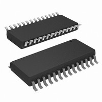
IC PIC MCU 16KB FLASH 28SOIC
Manufacturer
Microchip Technology
Series
PIC® XLP™ 18Fr
Datasheets
1.PIC16F722-ISS.pdf
(8 pages)
2.PIC18F26J13-ISS.pdf
(496 pages)
3.PIC18F24K22-ISP.pdf
(494 pages)
Specifications of PIC18F24K22-I/SO
Core Size
8-Bit
Program Memory Size
16KB (8K x 16)
Core Processor
PIC
Speed
64MHz
Connectivity
I²C, SPI, UART/USART
Peripherals
Brown-out Detect/Reset, HLVD, POR, PWM, WDT
Number Of I /o
24
Program Memory Type
FLASH
Eeprom Size
256 x 8
Ram Size
768 x 8
Voltage - Supply (vcc/vdd)
1.8 V ~ 5.5 V
Data Converters
A/D 19x10b
Oscillator Type
Internal
Operating Temperature
-40°C ~ 85°C
Package / Case
28-SOIC (0.300", 7.50mm Width)
Controller Family/series
PIC18
No. Of I/o's
25
Eeprom Memory Size
256Byte
Ram Memory Size
768Byte
Cpu Speed
64MHz
No. Of Timers
7
Lead Free Status / RoHS Status
Lead free / RoHS Compliant
Available stocks
Company
Part Number
Manufacturer
Quantity
Price
Company:

Part Number:
PIC18F24K22-I/SO
Manufacturer:
MICRON
Quantity:
12


18.8
There are four additional comparator features:
• Simultaneous read of comparator outputs
• Internal reference selection
• Hysteresis selection
• Output Synchronization
18.8.1
The MC1OUT and MC2OUT bits of the CM2CON1
register are mirror copies of both comparator outputs.
The ability to read both outputs simultaneously from a
single register eliminates the timing skew of reading
separate registers.
18.8.2
There are two internal voltage references available to
the non-inverting input of each comparator. One of
these is the Fixed Voltage Reference (FVR) and the
other is the variable Digital-to-Analog Converter (DAC).
The CxRSEL bit of the CM2CON1 register determines
which of these references is routed to the Comparator
Voltage reference output (C
the comparator is accomplished by the CxR bit of the
CMxCON0 register. See Section 21.0 “Fixed Voltage
Reference (FVR)” and Figure 18-2 for more detail.
2010 Microchip Technology Inc.
Note 1: Obtaining the status of C1OUT or C2OUT
Additional Comparator Features
SIMULTANEOUS COMPARATOR
OUTPUT READ
INTERNAL REFERENCE
SELECTION
by reading CM2CON1 does not affect the
comparator interrupt mismatch registers.
X
V
REF
). Further routing to
Preliminary
18.8.3
Each Comparator has a selectable hysteresis feature.
The hysteresis can be enabled by setting the CxHYS
bit of the CM2CON1 register. See Section 27.0 “Elec-
trical Characteristics” for more details.
18.8.4
The Comparator Cx output can be synchronized with
Timer1 by setting the CxSYNC bit of the CM2CON1
register. When enabled, the Cx output is latched on
the falling edge of the Timer1 source clock. If a
prescaler is used with Timer1, the comparator output
is latched after the prescaling function. To prevent a
race condition between the Timer1 clock and Timer1
gate, Timer1 increments on the rising edge of its clock
source, and the falling edge latches the comparator
output.
(Figure 18-2)
(Figure 12-1) for more information.
PIC18(L)F2X/4XK22
See
COMPARATOR HYSTERESIS
SYNCHRONIZING COMPARATOR
OUTPUT TO TIMER1
and
the
the
Comparator
Timer1
DS41412A-page 315
Block
Block
Diagram
Diagram
Related parts for PIC18F24K22-I/SO
Image
Part Number
Description
Manufacturer
Datasheet
Request
R

Part Number:
Description:
Manufacturer:
Microchip Technology Inc.
Datasheet:
Part Number:
Description:
Manufacturer:
Microchip Technology Inc.
Datasheet:
Part Number:
Description:
Manufacturer:
Microchip Technology Inc.
Datasheet:
Part Number:
Description:
Manufacturer:
Microchip Technology Inc.
Datasheet:
Part Number:
Description:
Manufacturer:
Microchip Technology Inc.
Datasheet:
Part Number:
Description:
Manufacturer:
Microchip Technology Inc.
Datasheet:
Part Number:
Description:
Manufacturer:
Microchip Technology Inc.
Datasheet:
Part Number:
Description:
Manufacturer:
Microchip Technology Inc.
Datasheet: