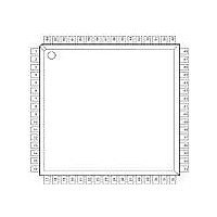
XRT5894IV-F Exar Corporation, XRT5894IV-F Datasheet - Page 11

XRT5894IV-F
Manufacturer Part Number
XRT5894IV-F
Description
IC LIU E1 QUAD 64TQFP
Manufacturer
Exar Corporation
Datasheet
1.XRT5894IVTR-F.pdf
(19 pages)
Specifications of XRT5894IV-F
Maximum Operating Temperature
+ 85 C
Maximum Power Dissipation
590 mW / 1240 mW
Minimum Operating Temperature
- 40 C
Mounting Style
SMD/SMT
Operating Supply Voltage
3.3 V / 5 V
Package / Case
TQFP-64
Supply Voltage Range
3.135V To 3.465V, 4.75V To 5.25
Power Dissipation Pd
1240mW
Operating Temperature Range
-40°C To +85°C
Digital Ic Case Style
TQFP
No. Of Pins
64
Filter Terminals
SMD
Rohs Compliant
Yes
Lead Free Status / RoHS Status
Lead free / RoHS Compliant
Lead Free Status / RoHS Status
Lead free / RoHS Compliant, Lead free / RoHS Compliant
Available stocks
Company
Part Number
Manufacturer
Quantity
Price
Company:
Part Number:
XRT5894IV-F
Manufacturer:
EXAR
Quantity:
1 558
Company:
Part Number:
XRT5894IV-F
Manufacturer:
Exar Corporation
Quantity:
10 000
Part Number:
XRT5894IV-F
Manufacturer:
EXAR/艾科嘉
Quantity:
20 000
SYSTEM DESCRIPTION
This device is a four channel E1 transceiver that provides
an electrical interface for 2.048Mbps applications. Its
unique architecture includes four receiver circuits that
convert ITU G.703 compliant bipolar signals to TTL
compatible logic levels. Each receiver includes a LOS
(Loss of Signal) detection circuit that may be configured
for either a fixed or a user-programmable LOS response
time delay.
transmitters convert TTL compatible logic levels to G.703
compatible bipolar signals. Each transmitter may be
operated either with RZ, or NRZ data types. In NRZ mode
a transmit clock is required as well.
description applies to any of the four receivers or
transmitters contained in the XRT5894. Therefore, the
suffix numbers for a particular channel are deleted for
simplicity. i.e. “RTIP” applies to RTIP1 through RTIP4.
Receiver Operation
A bipolar signal is transformer-coupled to the receiver
differential inputs (RTIP and RRING). The receiver is able
to tolerate up to 12dB of line loss measured at 1.024MHz.
It contains slicing circuitry that automatically samples the
incoming data at a fixed percentage (50% nominal) of the
peak signal amplitude. A precision peak detector
maintains the slicing level accuracy. The TTL compatible
receiver output data rails appear at the RXPOS and
RXNEG pins. The pulse width of this data; which is in RZ
format, is a function of the amount of the cable loss
present.
Receiver Loss Of Signal Detection (LOS)
Absence of signal at any receiver input is detected by the
loss of signal (LOS) circuit. One LOS detection circuitry is
provisioned for each receiver. The LOS signal is asserted
(LOS=1) when a LOS condition is detected and is cleared
(LOS=0) when a valid input signal is restored.
Two modes of LOS circuit operation are supported.
These distinct modes are called “automatic” and
“user-programmable”. When LOSSEL (pin 25) is set to
logic “1”, the automatic mode is selected. In this mode the
LOS condition will be declared and cleared in full
compliance with ITU G.775 specification. When LOSSEL
is connected to logic “0”, the user-programmable delay
mode is enabled. In this mode the user has the option of
extending the delay of LOS declaration and clearing
Rev. 1.10
Similarly, in the transmit direction, four
The following
11
specified in the ITU G.775. This is done by providing a
user-supplied clock to LOSCNT (pin 45). The “user
programmable mode” is provisioned to allow systems
designers to comply with older versions of LOS
specifications in legacy systems. It needs to be stressed
that the delay for declaration and clearing of the LOS
condition will never be less than the range specified in the
G.775 specification (10-255 pulse intervals).
The LOS detection/clearing circuitry of the XRT5894 in
“automatic” mode will detect LOS when the incoming
signal has “no transitions” i.e. when the signal level is less
than or equal to a signal level A
level, for N consecutive pulse intervals, where 10<N<255.
The value of A
depending on the ones density of the incoming signal
assuming the received data has minimum permissible
ones density. Furthermore LOS detect is cleared when
the incoming signal has “transitions,” i.e. when the signal
level is greater than or equal to a signal level of A
below nominal, for N consecutive pulse intervals, where
10<N<255. The value of A
31dB depending on the ones density of the incoming
signal assuming the received data has minimum
permissible ones density. Each pulse interval is 488ns at
E1 rates. The absolute value of A
A
The LOS detection/clearing criteria described above is
fully compliant with G.775 LOS specification. In the “user
programmable” mode the user has the option of
extending the declaration and clearing delay (10<N<255)
by an amount which is equal to 2048 x T. T is the time
period of the clock supplied to LOSCNT (pin 45) by the
user.
Nominal signal level is defined as 2.37V peak measured
between RTIP or RRING and ground. (This voltage will
be present in 75W applications using a 1:2 CT ratio input
transformer terminated in 300W with the center tap
grounded with 0dB of cable and a 2.37V peak amplitude
transmit pulse at the cable input.)
Transmitters
This device contains four identical ITU G.703 compliant
transmitters. The output stage of each transmitter is a
differential voltage driver. External resistors need to be
connected to the primary of output transformer. This is
necessary to maintain an accurate source impedance
D
by at least 1dB.
D
can vary between 10dB to 32dB
C
can vary between 9dB to
D
dB below nominal signal
C
is always smaller than
C
dB


