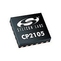
CP2105-F01-GM Silicon Laboratories Inc, CP2105-F01-GM Datasheet - Page 11

CP2105-F01-GM
Manufacturer Part Number
CP2105-F01-GM
Description
IC SGL USB-DL UART BRIDGE 24QFN
Manufacturer
Silicon Laboratories Inc
Specifications of CP2105-F01-GM
Package / Case
24-WFQFN Exposed Pad
Applications
UART-to-USB Bridge
Interface
UART, USB
Voltage - Supply
1.8V, 3 V ~ 3.6 V
Mounting Type
Surface Mount
Input Voltage Range (max)
3.6 V
Maximum Operating Temperature
+ 85 C
Minimum Operating Temperature
- 40 C
Mounting Style
SMD/SMT
Operating Supply Voltage
3.3 V
Supply Current (max)
18.5 mA
Lead Free Status / RoHS Status
Lead free / RoHS Compliant
For Use With
336-2005 - KIT EVAL FOR CP2105
Lead Free Status / Rohs Status
Lead free / RoHS Compliant
Other names
336-2009-5
Available stocks
Company
Part Number
Manufacturer
Quantity
Price
Company:
Part Number:
CP2105-F01-GM
Manufacturer:
Silicon
Quantity:
3 015
Part Number:
CP2105-F01-GMR
Manufacturer:
SILICON LABS/芯科
Quantity:
20 000
Notes:
General
Solder Mask Design
Stencil Design
Card Assembly
Dimension
1. All dimensions shown are in millimeters (mm) unless otherwise noted.
2. This Land Pattern Design is based on the IPC-7351 guidelines.
3. All metal pads are to be non-solder mask defined (NSMD). Clearance between the solder
4. A stainless steel, laser-cut and electro-polished stencil with trapezoidal walls should be used
5. The stencil thickness should be 0.125 mm (5 mils).
6. The ratio of stencil aperture to land pad size should be 1:1 for all perimeter pads.
7. A 2x2 array of 1.10 x 1.10 mm openings on a 1.30 mm pitch should be used for the center
8. A No-Clean, Type-3 solder paste is recommended.
9. The recommended card reflow profile is per the JEDEC/IPC J-STD-020 specification for Small
C1
C2
X1
E
mask and the metal pad is to be 60 m minimum, all the way around the pad.
to assure good solder paste release.
pad.
Body Components.
Figure 4. QFN-24 Recommended PCB Land Pattern
Table 9. QFN-24 PCB Land Pattern Dimensions
3.90
3.90
0.20
Min
0.50 BSC
Max
4.00
4.00
0.30
Rev. 1.0
Dimension
X2
Y1
Y2
2.70
0.65
2.70
Min
Max
2.80
0.75
2.80
CP2105
11


