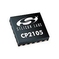
CP2105-F01-GM Silicon Laboratories Inc, CP2105-F01-GM Datasheet - Page 18

CP2105-F01-GM
Manufacturer Part Number
CP2105-F01-GM
Description
IC SGL USB-DL UART BRIDGE 24QFN
Manufacturer
Silicon Laboratories Inc
Specifications of CP2105-F01-GM
Package / Case
24-WFQFN Exposed Pad
Applications
UART-to-USB Bridge
Interface
UART, USB
Voltage - Supply
1.8V, 3 V ~ 3.6 V
Mounting Type
Surface Mount
Input Voltage Range (max)
3.6 V
Maximum Operating Temperature
+ 85 C
Minimum Operating Temperature
- 40 C
Mounting Style
SMD/SMT
Operating Supply Voltage
3.3 V
Supply Current (max)
18.5 mA
Lead Free Status / RoHS Status
Lead free / RoHS Compliant
For Use With
336-2005 - KIT EVAL FOR CP2105
Lead Free Status / Rohs Status
Lead free / RoHS Compliant
Other names
336-2009-5
Available stocks
Company
Part Number
Manufacturer
Quantity
Price
Company:
Part Number:
CP2105-F01-GM
Manufacturer:
Silicon
Quantity:
3 015
Part Number:
CP2105-F01-GMR
Manufacturer:
SILICON LABS/芯科
Quantity:
20 000
CP2105
10. Voltage Regulator
The CP2105 includes an on-chip 5 to 3.45 V voltage regulator. This allows the CP2105 to be configured as either a
USB bus-powered device or a USB self-powered device. A typical connection diagram of the device in a bus-
powered application using the regulator is shown in Figure 8. When enabled, the voltage regulator output appears
on the V
characteristics. If it is desired to use the regulator to provide V
connections from Figure 8 can be used, but connect REGIN to an on-board 5 V supply, and disconnect it from the
VBUS pin.
18
Connector
Note 1 : Avalanche transient voltage suppression diodes compatible with Full-speed USB should be
Note 2 : An external pull-up is not required, but can be added for noise immunity.
Note 3 : VIO can be connected directly to VDD or to a supply as low as 1.8 V to set the I/O interface
Note 4 : If configuration ROM is to be programmed via USB, a 4.7 F capacitor must be added
USB
VBUS
GND
DD
D+
D-
3.45 V Power
pin and can be used to power external devices. See Table 5 for the voltage regulator electrical
added at the connector for ESD protection. Use Littelfuse p/n SP0503BAHT or equivalent.
voltage.
between NC / DCD_ECI / VPP and ground. During a programming operation, the pin should
not be connected to other circuitry, and VDD must be at least 3.3 V.
1-5 F
Figure 8. Typical Bus-Powered Connection Diagram
Note 1
Note 3
0.1 F
1 F
VIO
VDD
REGIN
GND
VBUS
D+
D-
Rev. 1.0
CP2105
GPIO.0_SCI / DCD_SCI
GPIO.1_ECI / DSR_ECI
GPIO.2_SCI / DSR_SCI
GPIO.1_SCI / DTR_SCI
GPIO0_ECI / DTR_ECI
NC / DCD_ECI / VPP
SUSPEND / RI_ECI
SUSPEND / RI_SCI
DD
in a self-powered application, the same
RXD_ECI
RXD_SCI
RTS_ECI
CTS_ECI
TXD_ECI
TXD_SCI
RTS_SCI
CTS_SCI
RST
VIO
Enhanced
and GPIO
and GPIO
Standard
Signals
Signals
UART
UART
Note 2
4.7 k
Note 4


